
Semiconductor Electronics Class 12 Notes - IIT JEE | NEET

eSaral Academic and Editorial Team
Summary
Semiconductor Electronics Class 12 Notes cover conductors, semiconductors and insulators, energy bands, intrinsic and extrinsic semiconductors, the p-n junction diode and its I–V characteristics, rectifiers, the Zener diode, LED, photodiode and solar cell, and logic gates. This page gives the formulas, truth tables, solved examples and handwritten notes, and it shows which topics each exam includes.
Semiconductor Electronics: Materials, Devices and Simple Circuits is Chapter 14 of NCERT Class 12 Physics, and it is the last chapter of the book. In the CBSE theory paper, it is the Electronic Devices unit, which carries 7 marks out of 70. The topics that each exam includes are different, so this page shows them first, and then explains every topic.
Semiconductor Electronics Class 12 Notes: Chapter Overview and Syllabus
Topic | CBSE 2026-27 | JEE Main 2026 (Unit 19) |
|---|---|---|
Energy bands (conductor, semiconductor, insulator) | Yes, qualitative ideas | Semiconductors |
p-n junction diode, I–V characteristics in forward and reverse bias | Yes | Yes |
Diode as a rectifier | Yes | Yes |
LED, photodiode, solar cell | Removed | Yes |
Zener diode and Zener diode as a voltage regulator | Removed | Yes |
Logic gates (OR, AND, NOT, NAND, NOR) | Removed | Yes |
Transistors, amplifiers | Removed | Not listed |
XOR gate | Not listed | Not listed |
Check the NMC syllabus for NEET, and the latest CBSE and NTA syllabi, before you decide which sections to learn. Sections marked “extra reading” below are outside the CBSE and JEE Main 2026 lists.
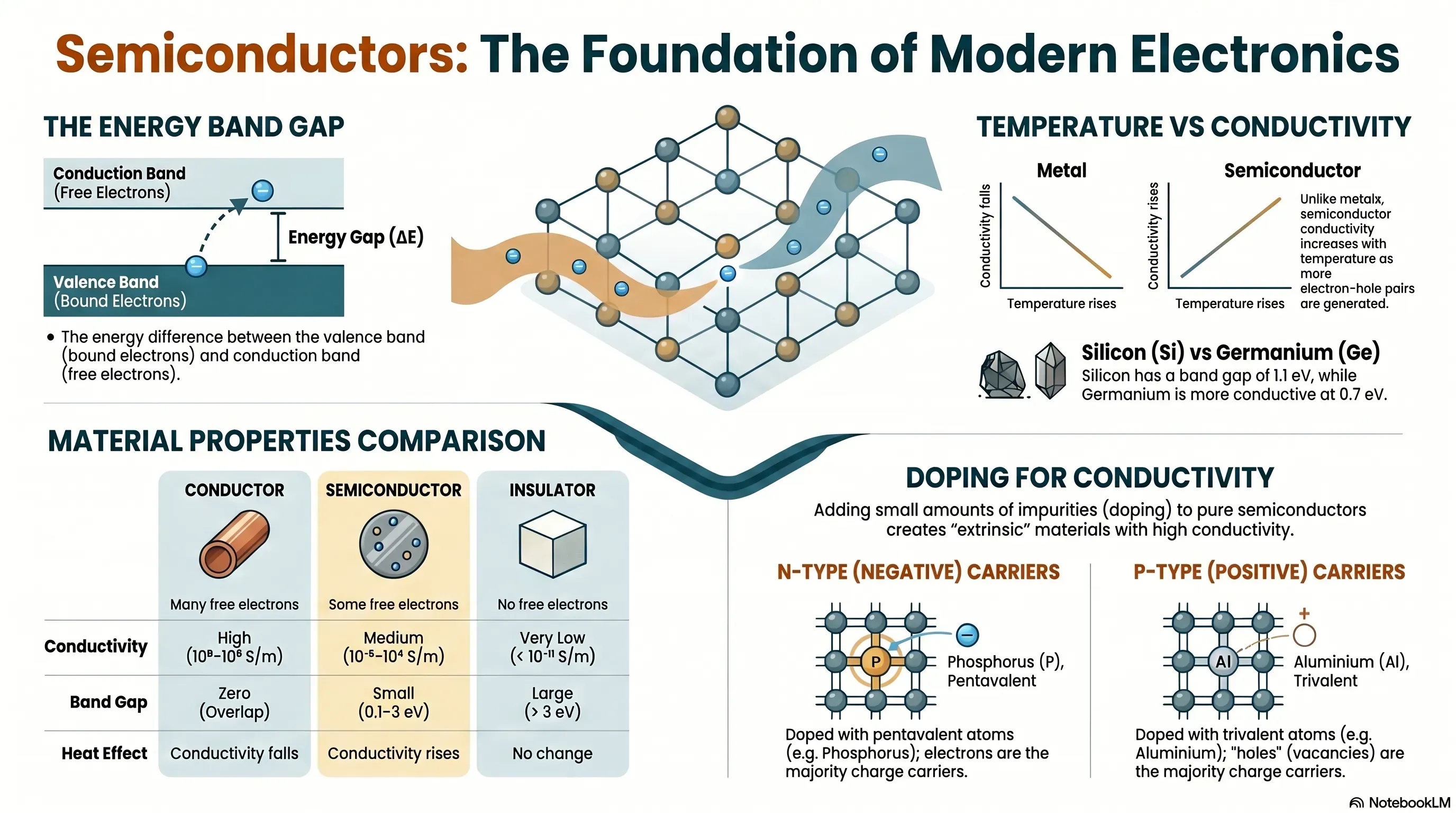
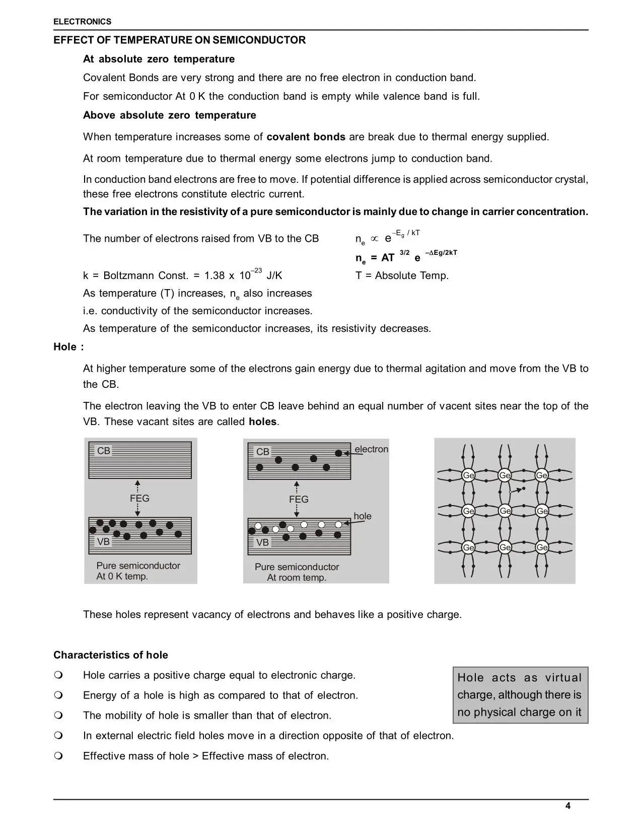
💡 Expert Tip by Saransh Gupta Sir, IIT Bombay AIR-41: In JEE Main, a very common question asks about the effect of temperature on conductivity. Always remember: in semiconductors, increasing temperature increases conductivity because more electron-hole pairs are generated. In metals, it's the opposite.
India's Best Exam Preparation for Class 12th - Download Now
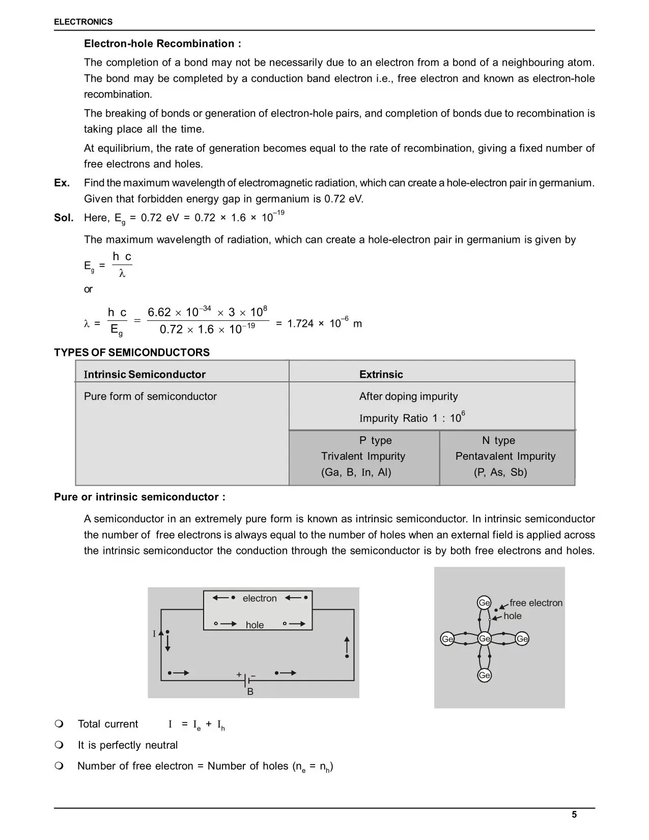
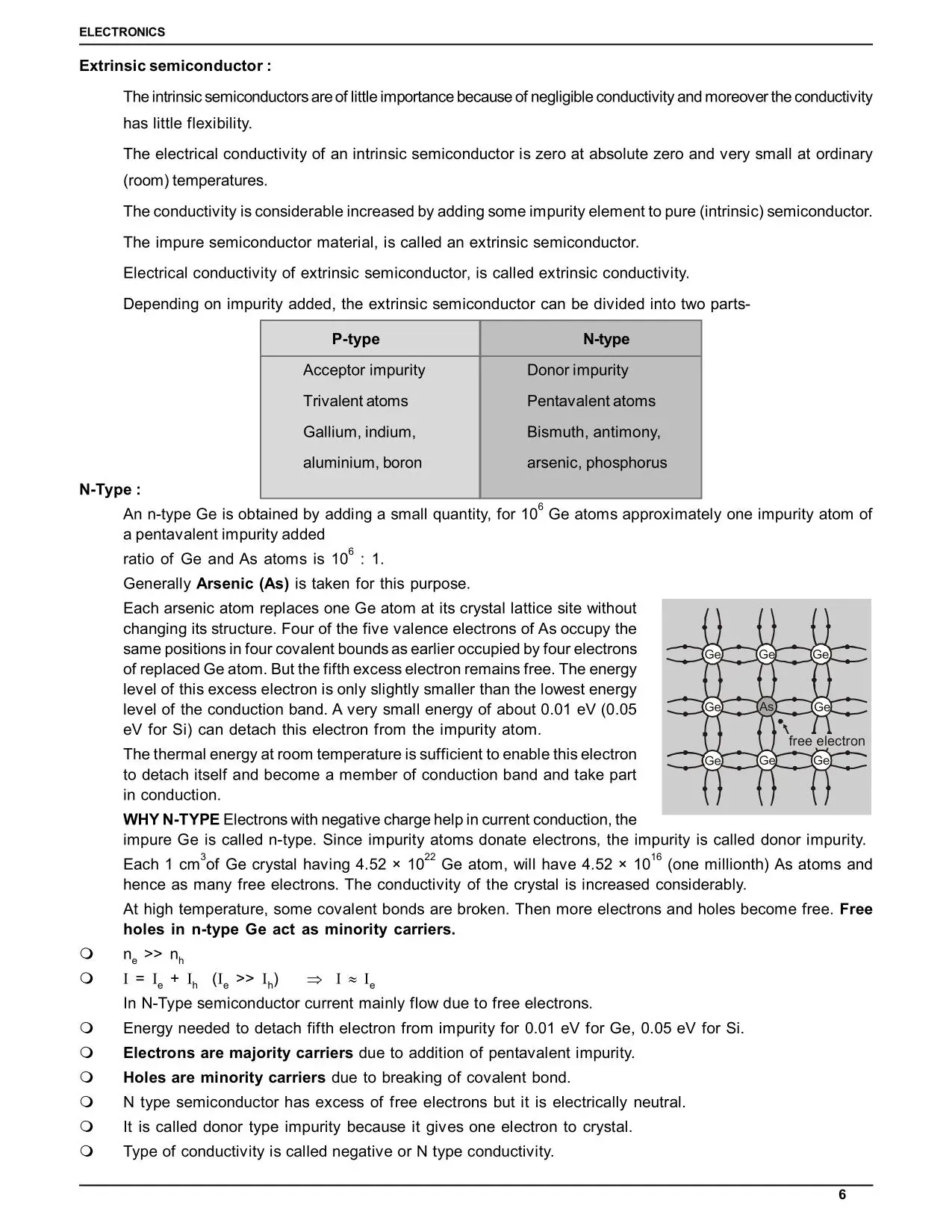
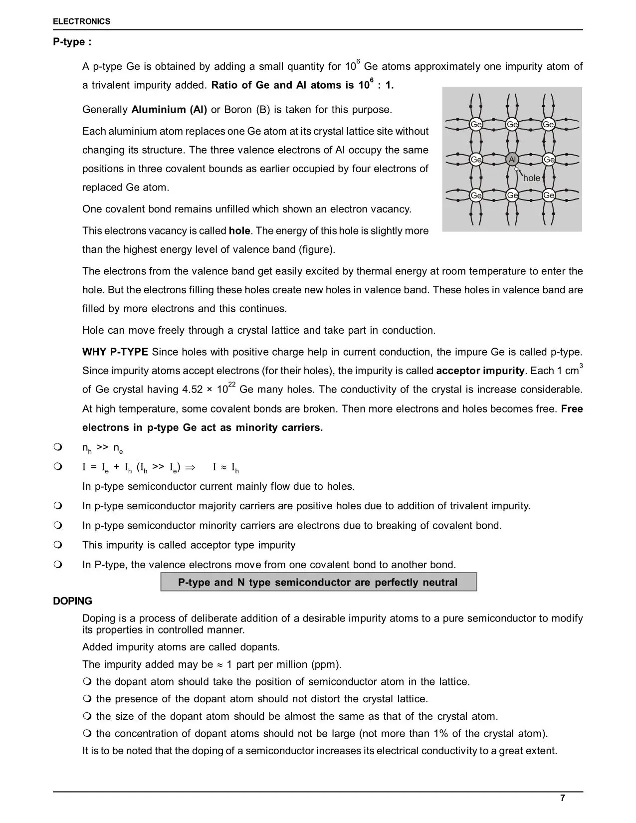
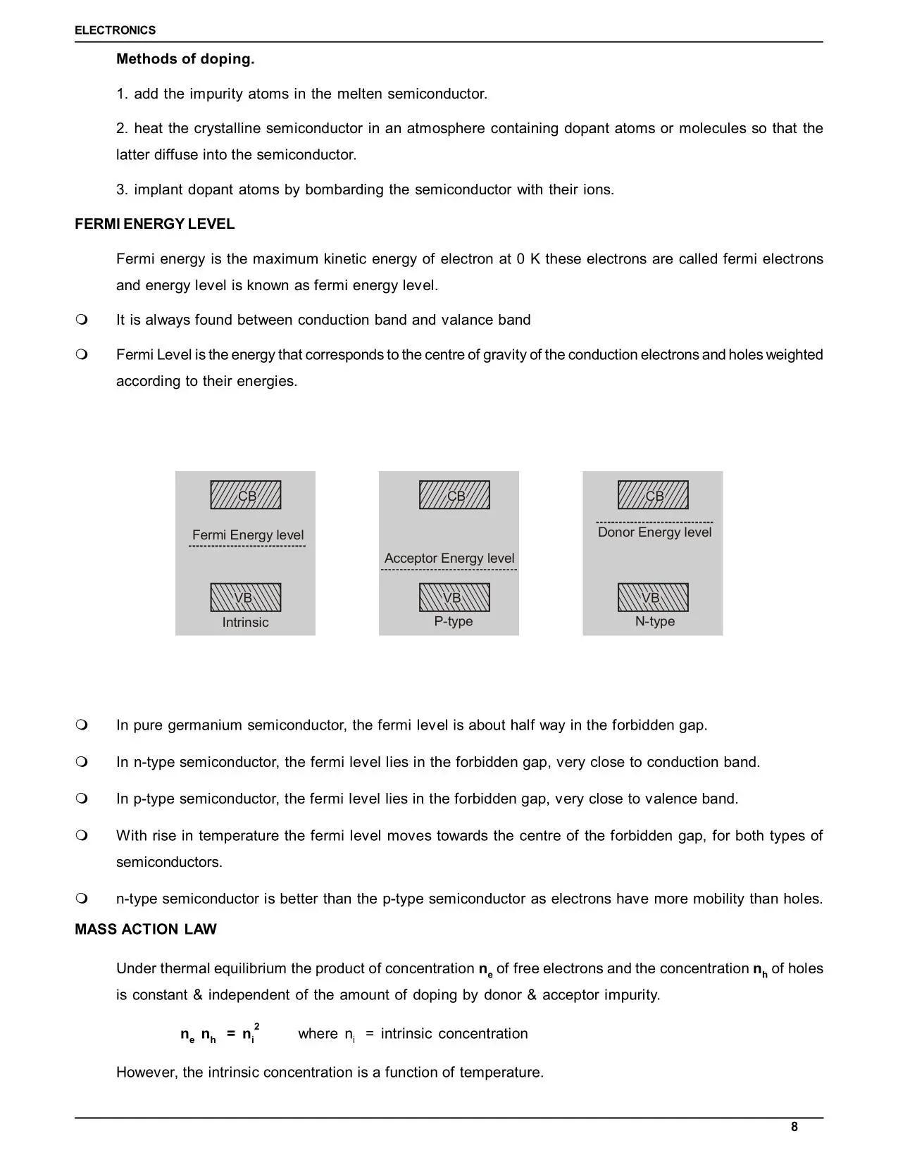
India's Best Exam Preparation for Class 12th - Download Now
India's Best Exam Preparation for Class 12th - Download Now
eSaral have already come up with an amazing Revision Series of Physics where you can easily revise your chapter within minutes with all the important formulae and key points. This revision series is free for all.
Click Here for Complete Physics Revision Series by Saransh Gupta Sir (AIR-41)
What Are Semiconductors in Semiconductor Electronics Class 12 Notes?
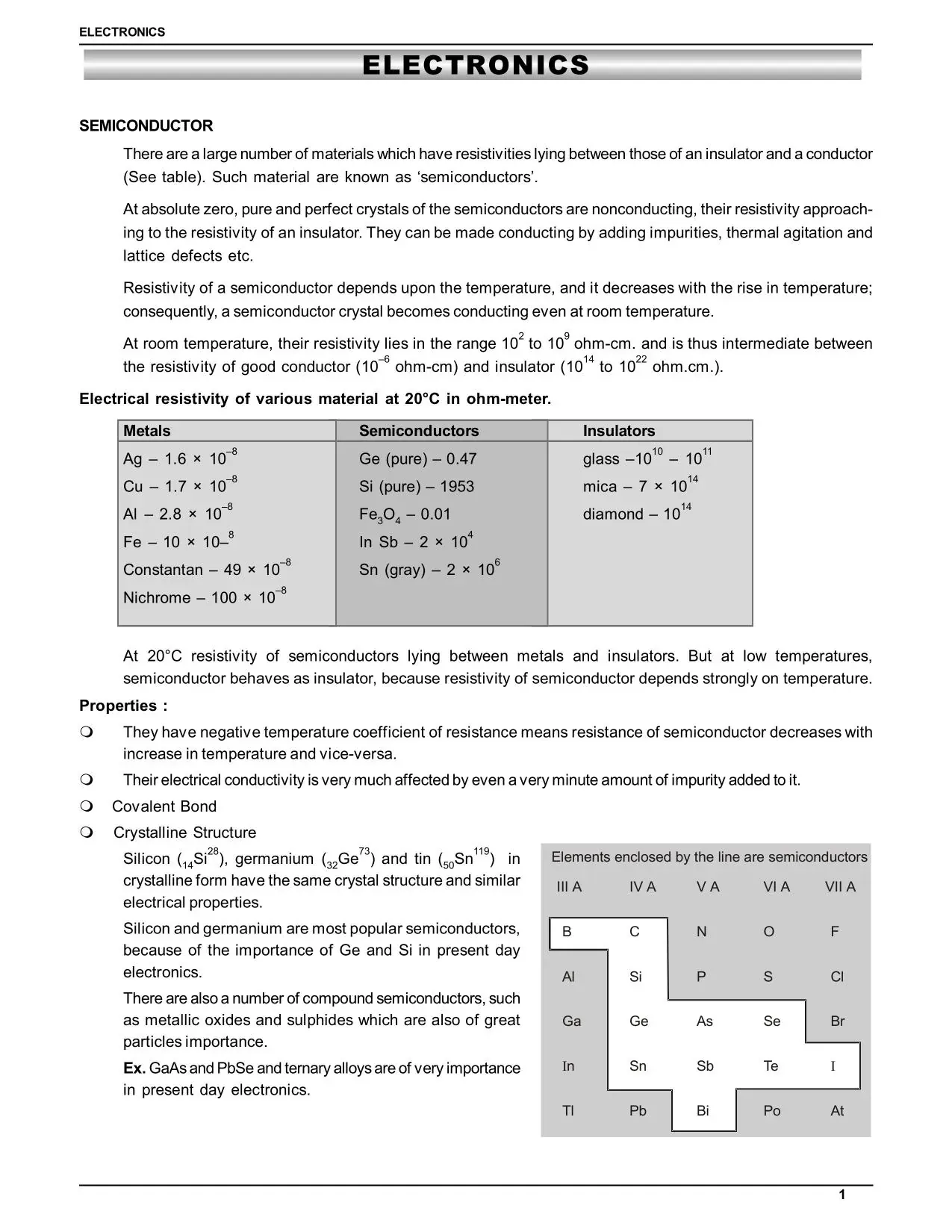
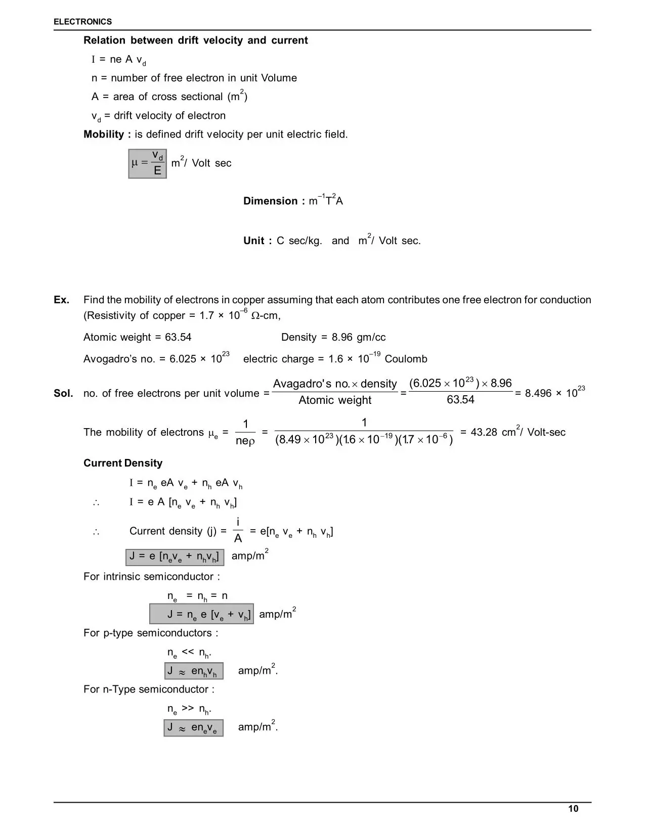
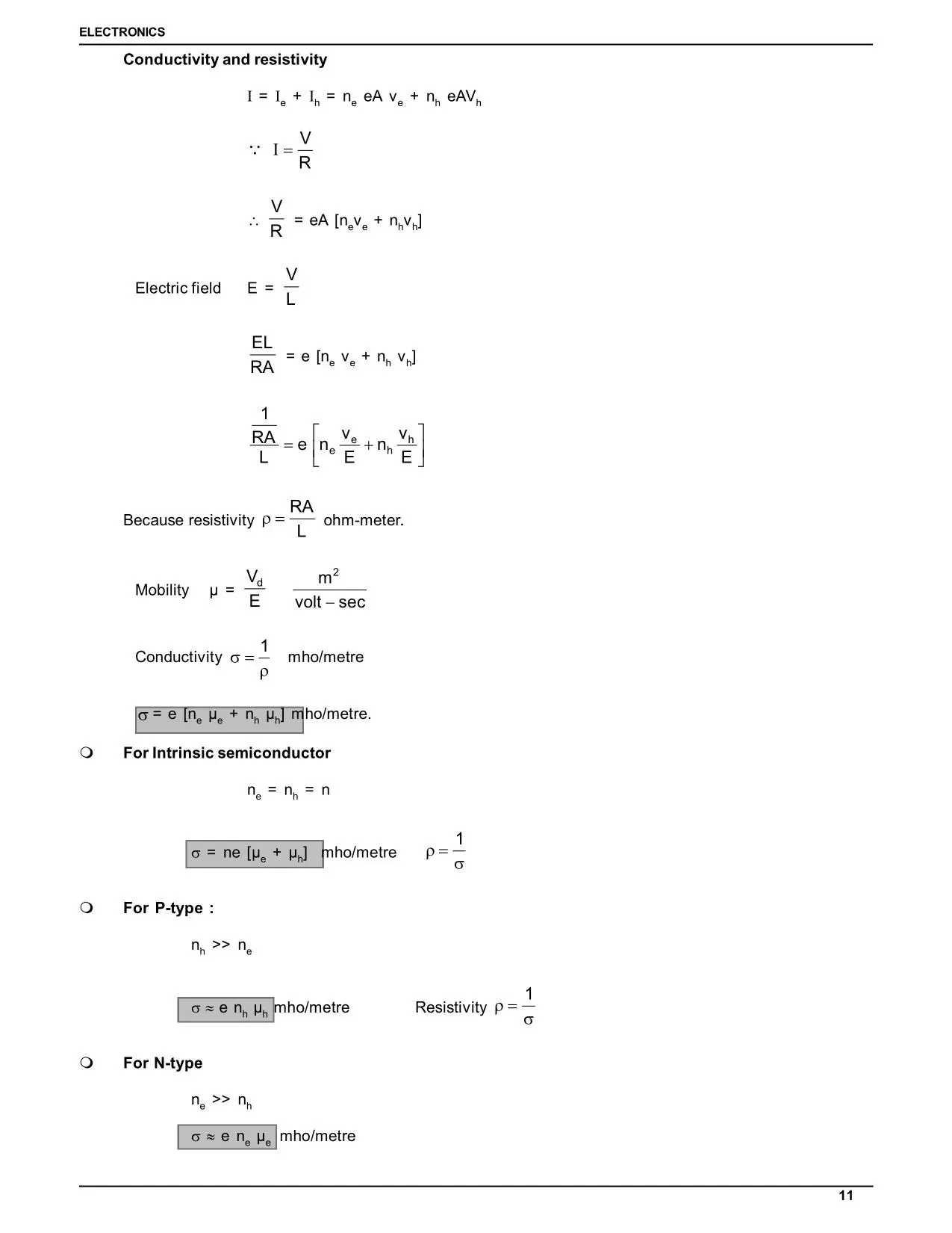
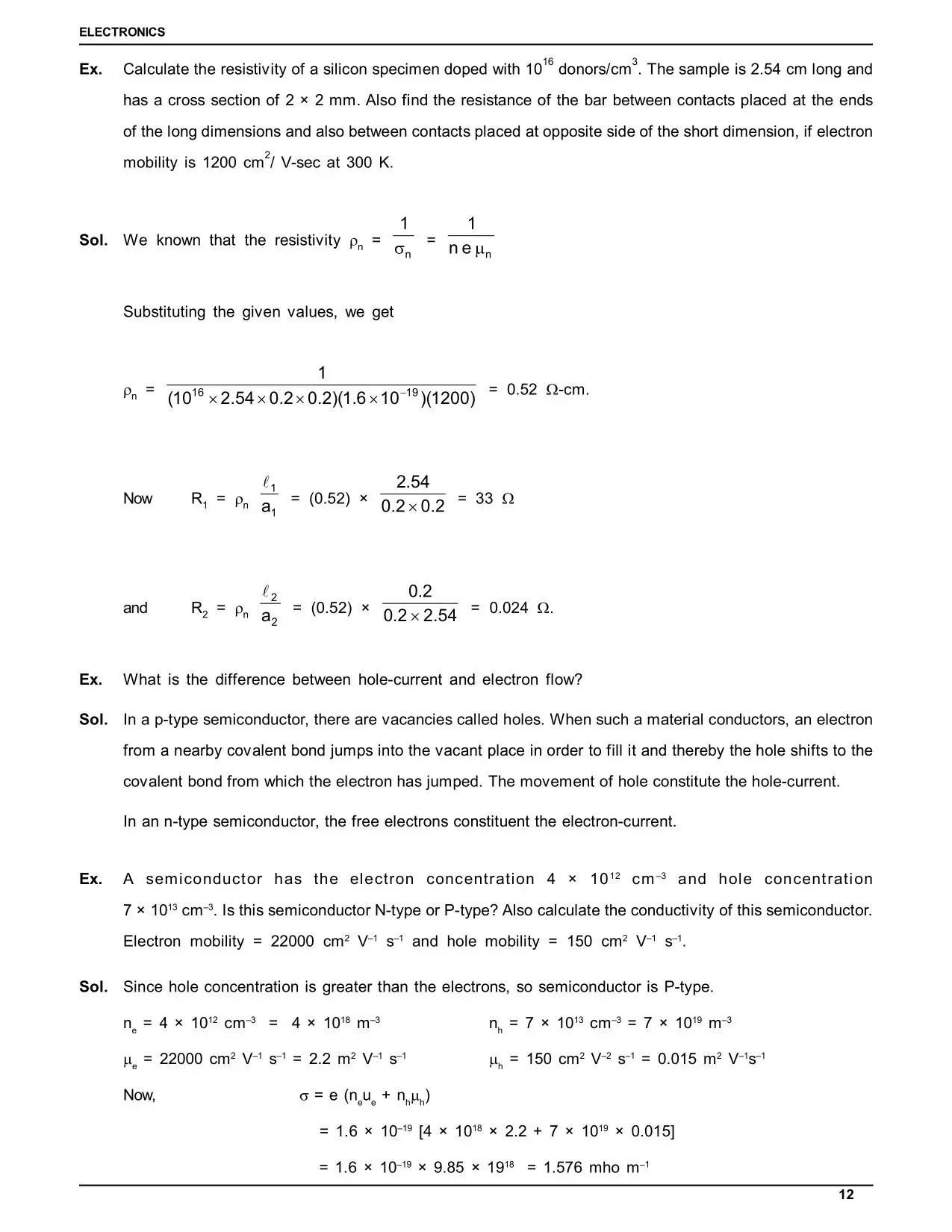
Semiconductors are materials whose electrical conductivity lies between that of conductors and insulators. Their conductivity increases with temperature, because more electrons gain enough energy to move to the conduction band. The most common examples are silicon (Si) and germanium (Ge).
Property | Conductor | Semiconductor | Insulator |
|---|---|---|---|
Conductivity | High ($10^{6}$ to $10^{8}$ S/m) | Medium (about $10^{-6}$ to $10^{4}$ S/m) | Very low (below $10^{-11}$ S/m) |
Band gap | Zero or bands overlap | Below about 3 eV | Above about 3 eV |
Effect of a rise in temperature | Conductivity decreases | Conductivity increases | Almost no change |
Example | Copper, silver | Silicon, germanium | Glass, rubber |
Energy Bands in Semiconductor Electronics Class 12 Notes
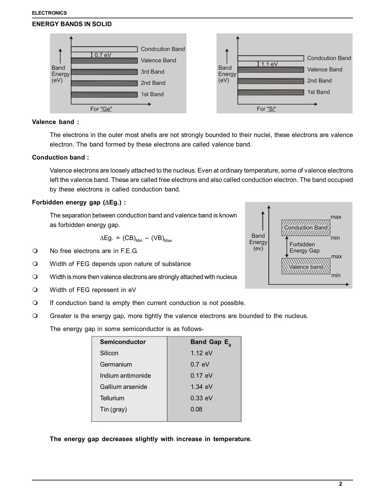
When many atoms form a solid, their discrete energy levels spread into energy bands.
- Valence band: the highest band that is filled with electrons at 0 K.
- Conduction band: the band above it, in which electrons are free to move and conduct.
- Forbidden gap (band gap) $E_g$: the energy difference between the two bands. No electron can have an energy in this gap.
The size of the gap decides the type of material:
- Conductor: the valence and conduction bands overlap, so $E_g \approx 0$.
- Semiconductor: a small gap, such as $E_g \approx 1.1$ eV for silicon and about $0.7$ eV for germanium.
- Insulator: a large gap, such as $E_g \approx 5.4$ eV for diamond.
When an electron moves from the valence band to the conduction band, it leaves a vacancy called a hole, which behaves like a positive charge carrier. In a semiconductor, both electrons and holes carry current.
Intrinsic and Extrinsic Semiconductors in Semiconductor Electronics Class 12 Notes
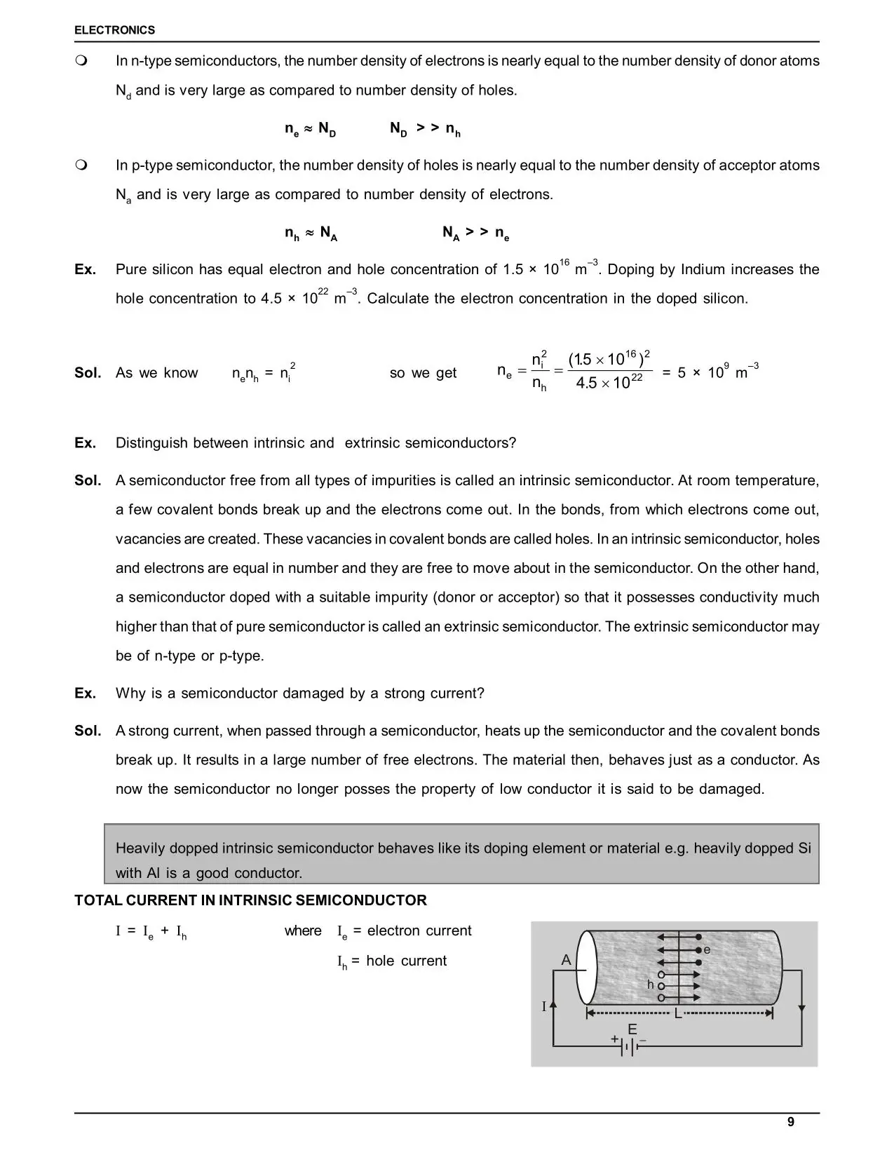
An intrinsic semiconductor is pure, and its electrons and holes come in pairs:
$$n_e = n_h = n_i$$
For any semiconductor in thermal equilibrium, the mass action law holds:
$$n_e\, n_h = n_i^{\,2}$$
An extrinsic semiconductor is made by doping a pure semiconductor with a small amount of an impurity.
Property | n-type | p-type |
|---|---|---|
Dopant | Pentavalent (P, As, Sb) | Trivalent (B, Al, In) |
Impurity atom is called | Donor | Acceptor |
Majority carriers | Electrons | Holes |
Minority carriers | Holes | Electrons |
Overall charge | Neutral | Neutral |
Both types are electrically neutral. The names n-type and p-type refer to the majority carrier, not to the overall charge.
P-N Junction Diode in Semiconductor Electronics Class 12 Notes
Formation of the Junction
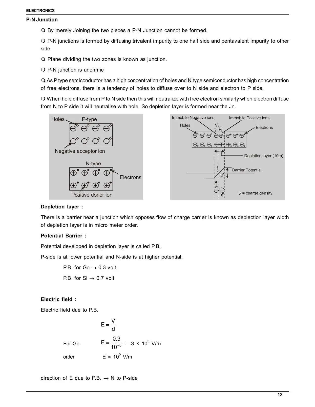
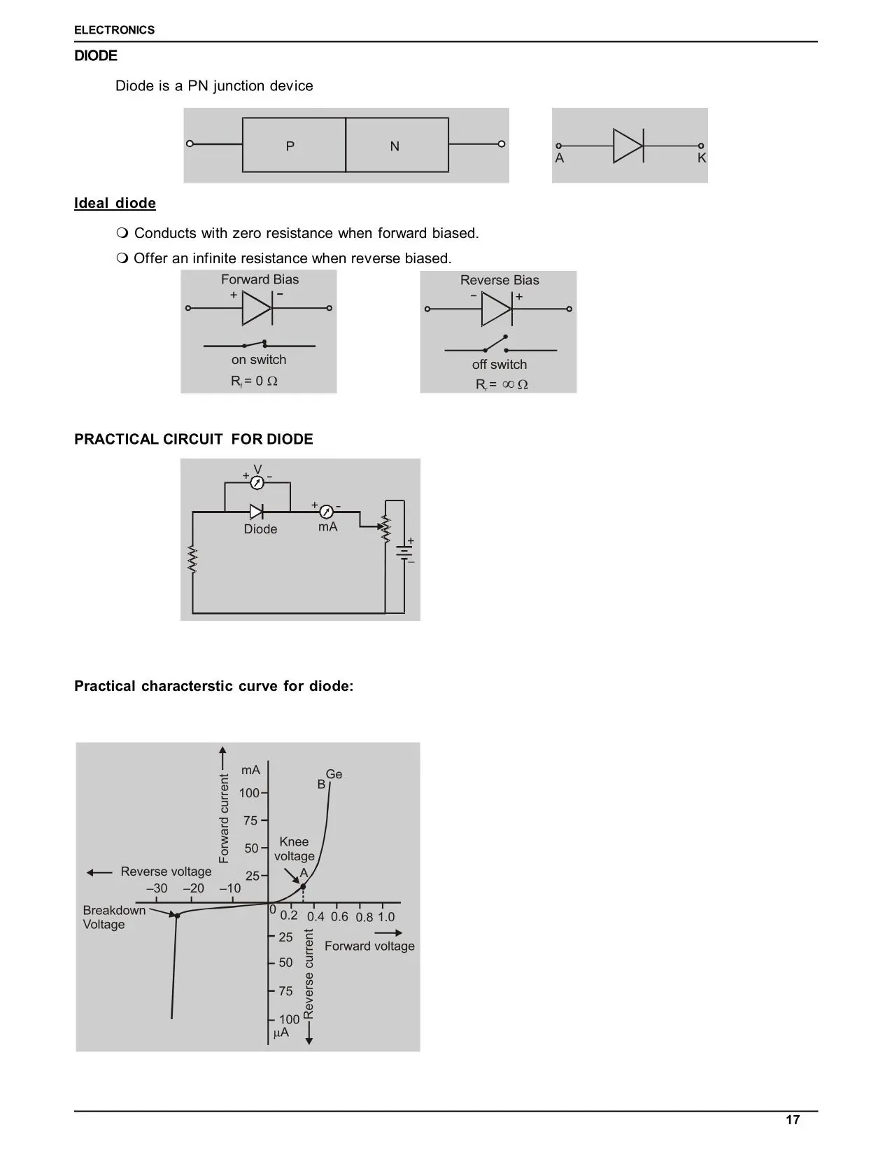
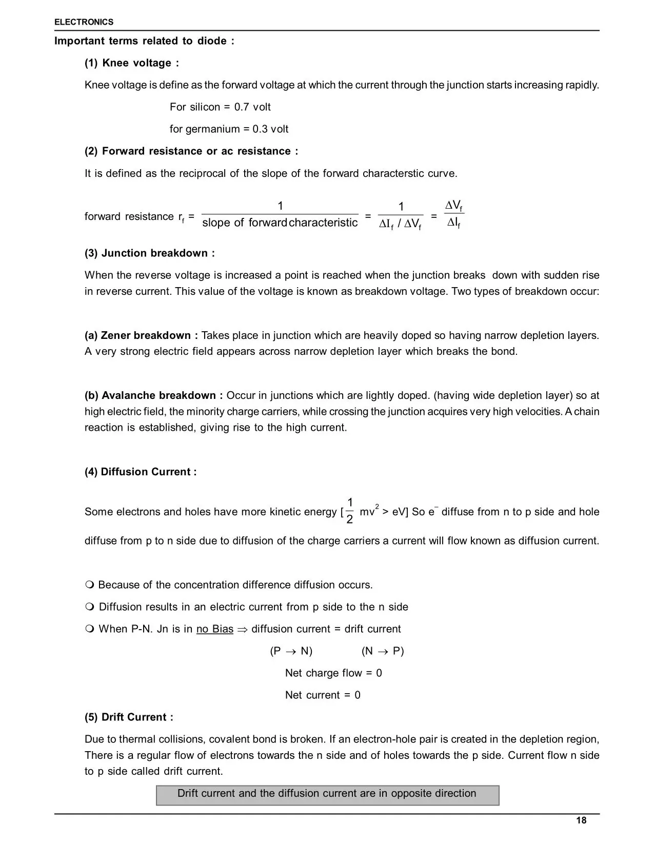
When a p-type and an n-type crystal are joined, electrons diffuse from the n-side to the p-side, and holes diffuse from the p-side to the n-side. This leaves immobile ions behind and forms a depletion layer, which is a region without mobile carriers. The layer creates a barrier potential, about $0.7$ V for silicon and about $0.3$ V for germanium. The barrier stops further diffusion, and it balances the drift current against the diffusion current.
Forward Bias and Reverse Bias
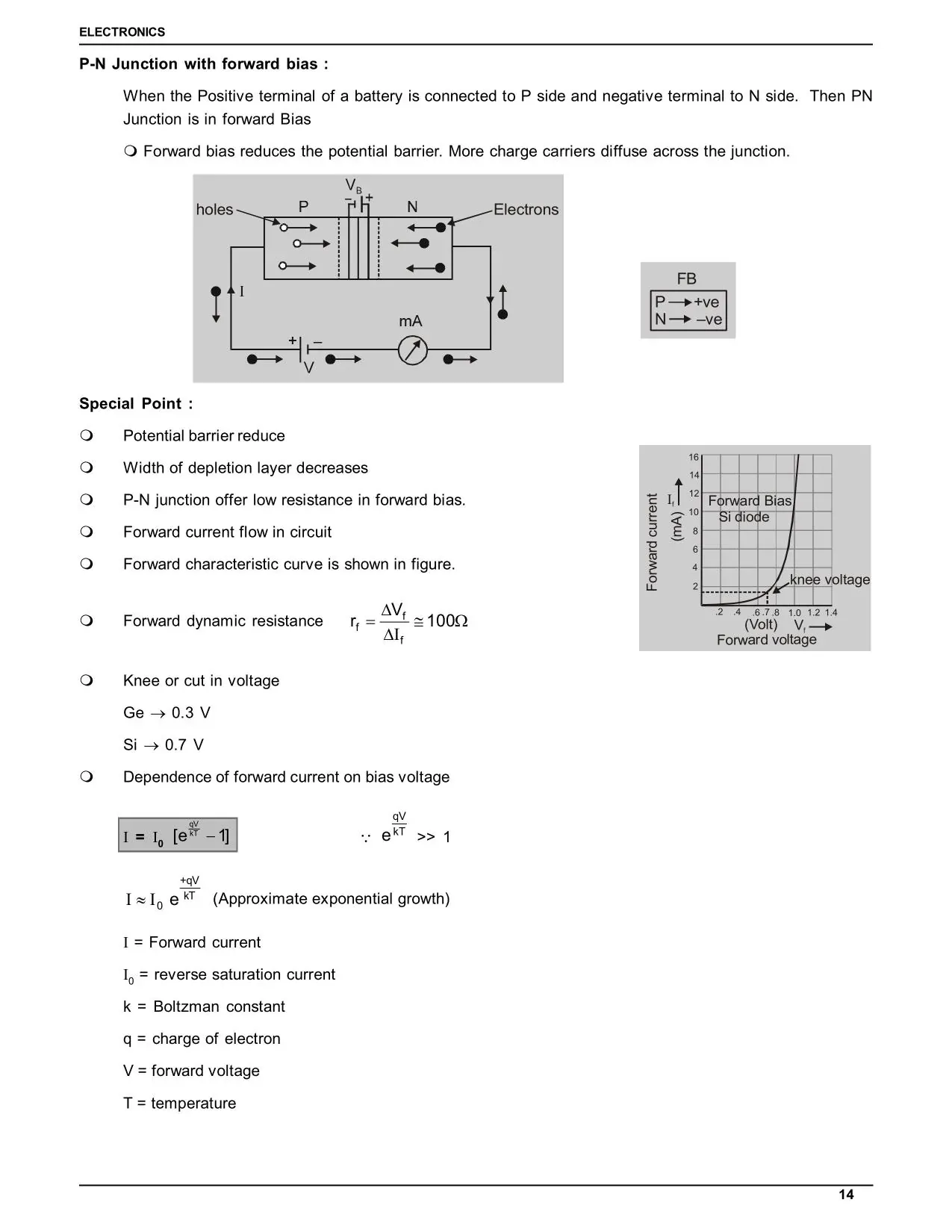
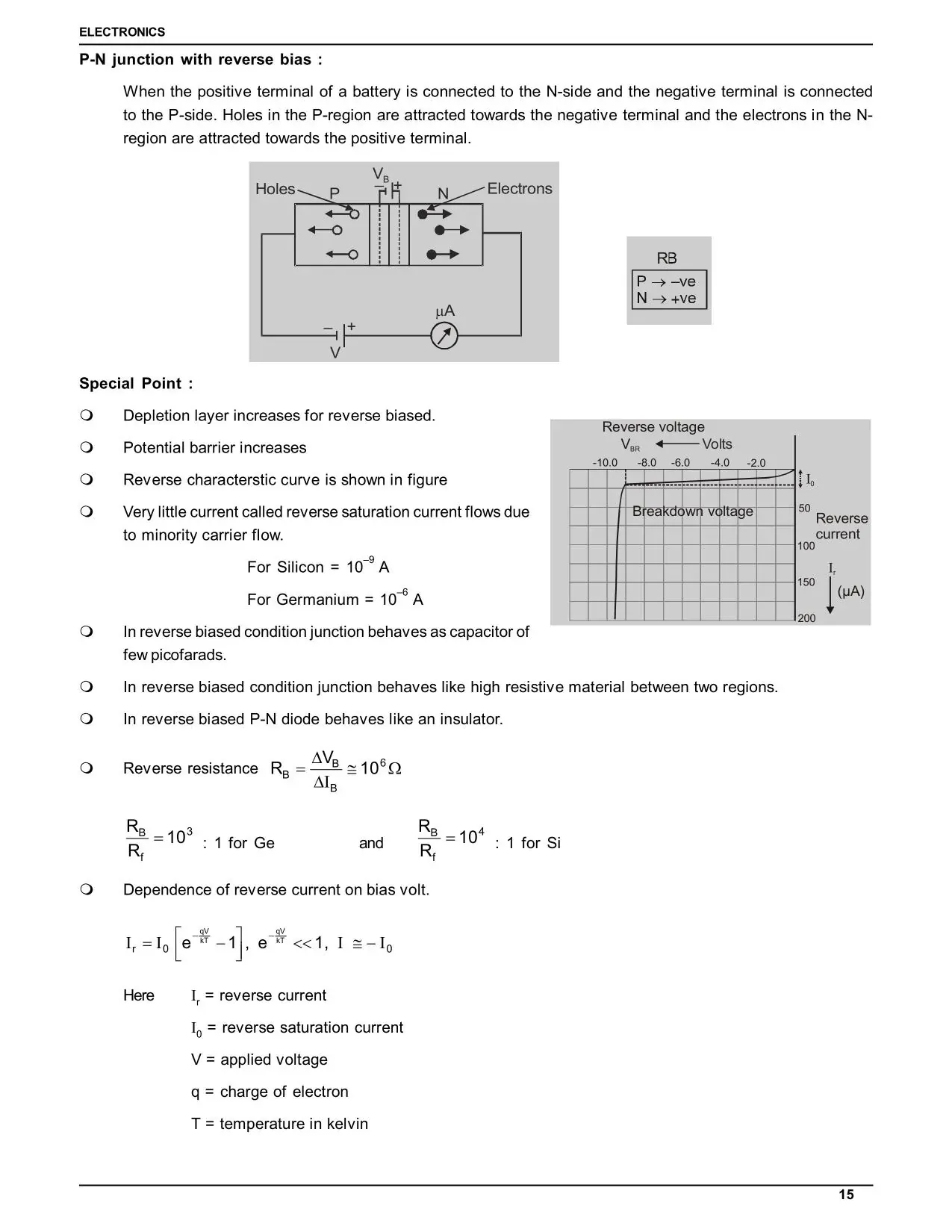
Feature | Forward bias | Reverse bias |
|---|---|---|
Connection | p-side to the positive terminal | p-side to the negative terminal |
External field vs barrier | Opposes the barrier | Adds to the barrier |
Depletion layer | Narrows | Widens |
Resistance | Low | Very high |
Current | Large above the knee voltage (mA range) | Very small reverse saturation current (μA range) |
In forward bias, the current rises sharply after the knee (threshold) voltage, about $0.7$ V for silicon and $0.3$ V for germanium. In reverse bias, a large enough voltage causes breakdown. The ratio of a small change in voltage to the resulting change in current is the dynamic resistance:
$$r_d = \frac{\Delta V}{\Delta I}$$
Diode as a Rectifier in Semiconductor Electronics Class 12 Notes
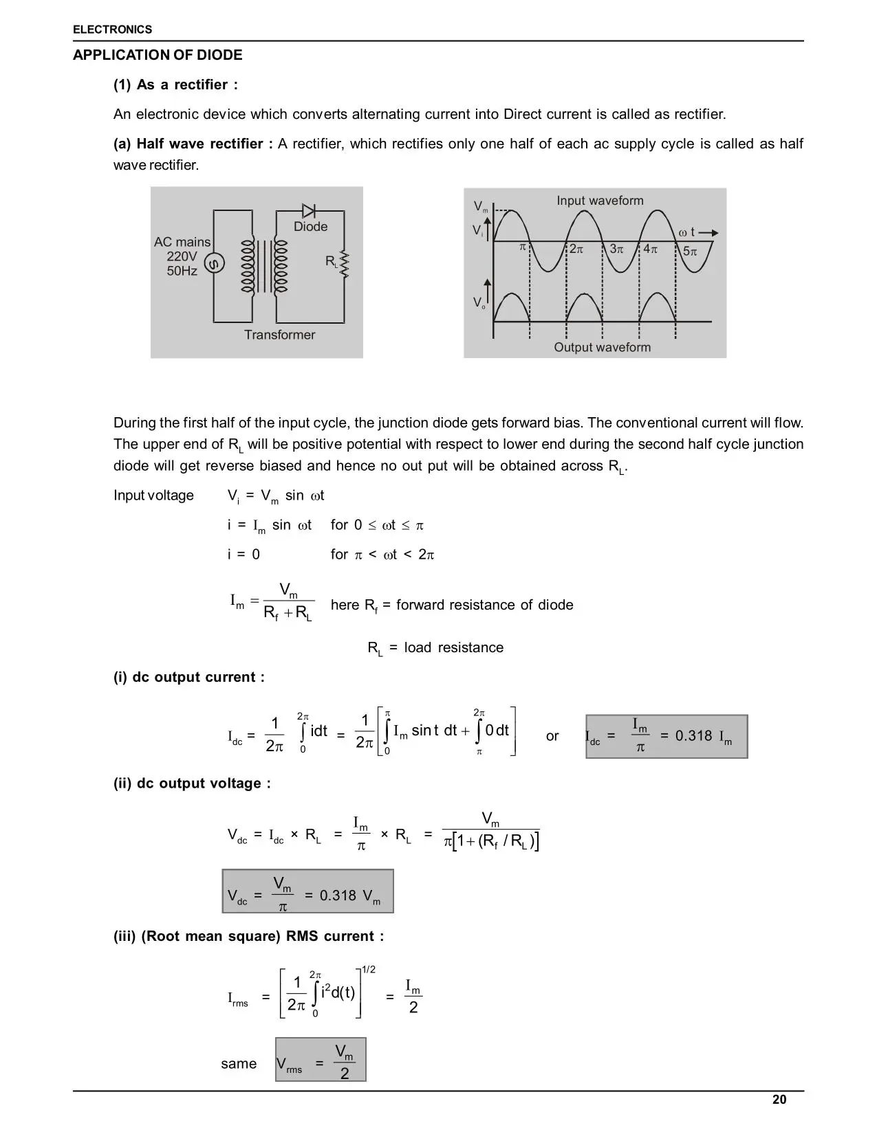
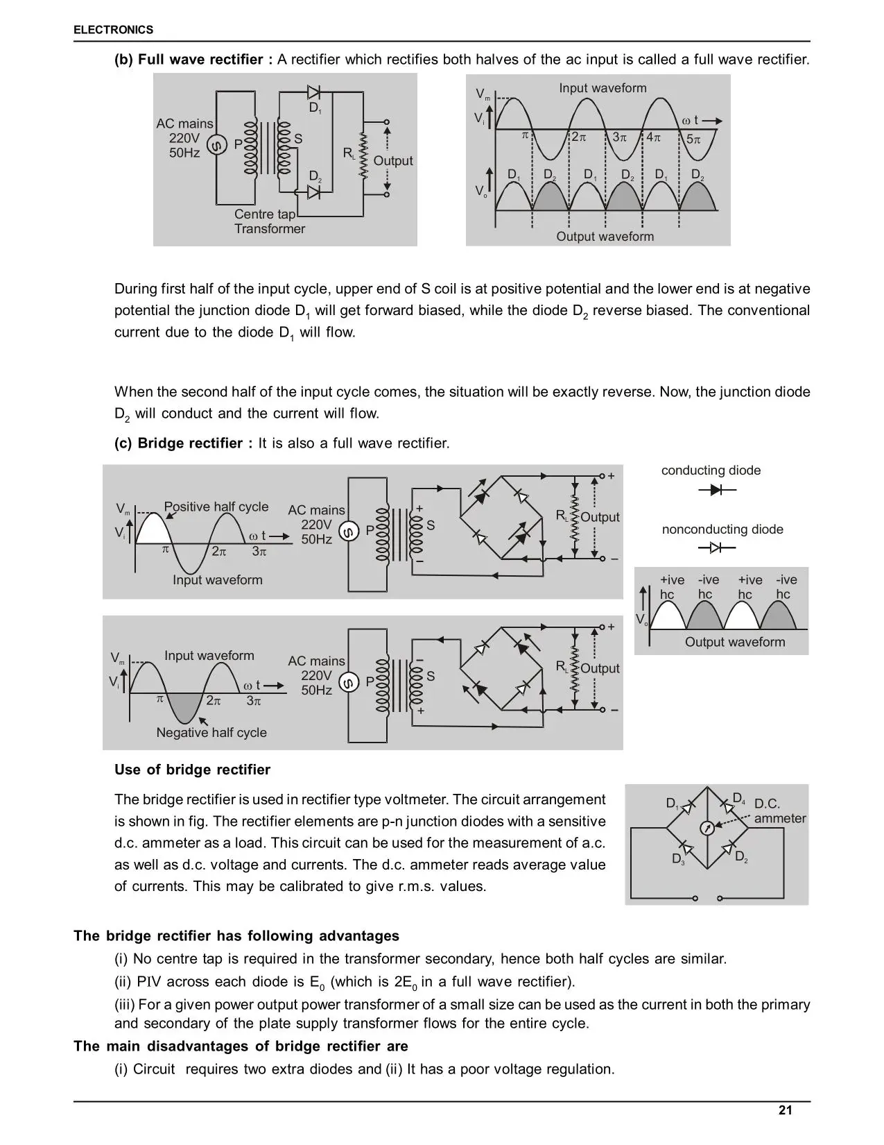
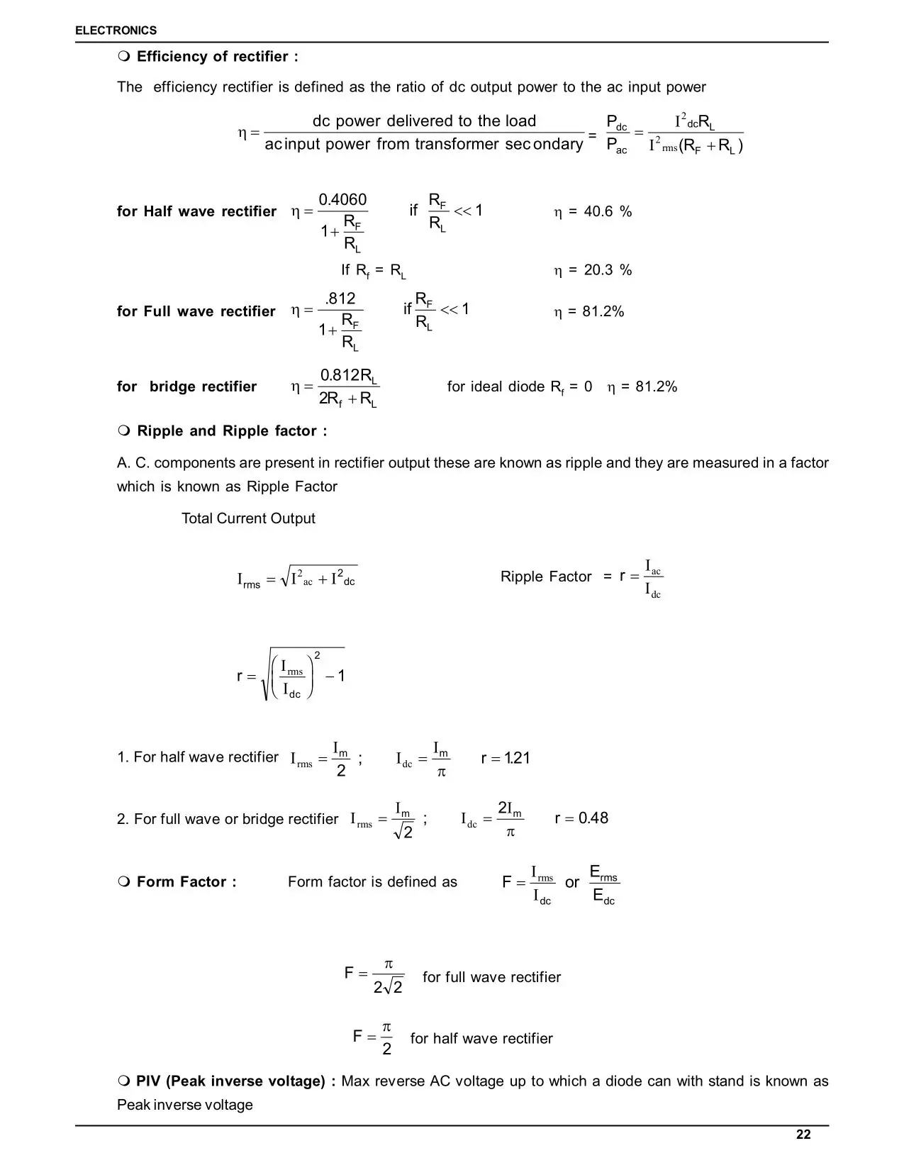
A rectifier changes an alternating voltage (AC) into a direct, one-way voltage (DC), because a diode conducts in forward bias only.
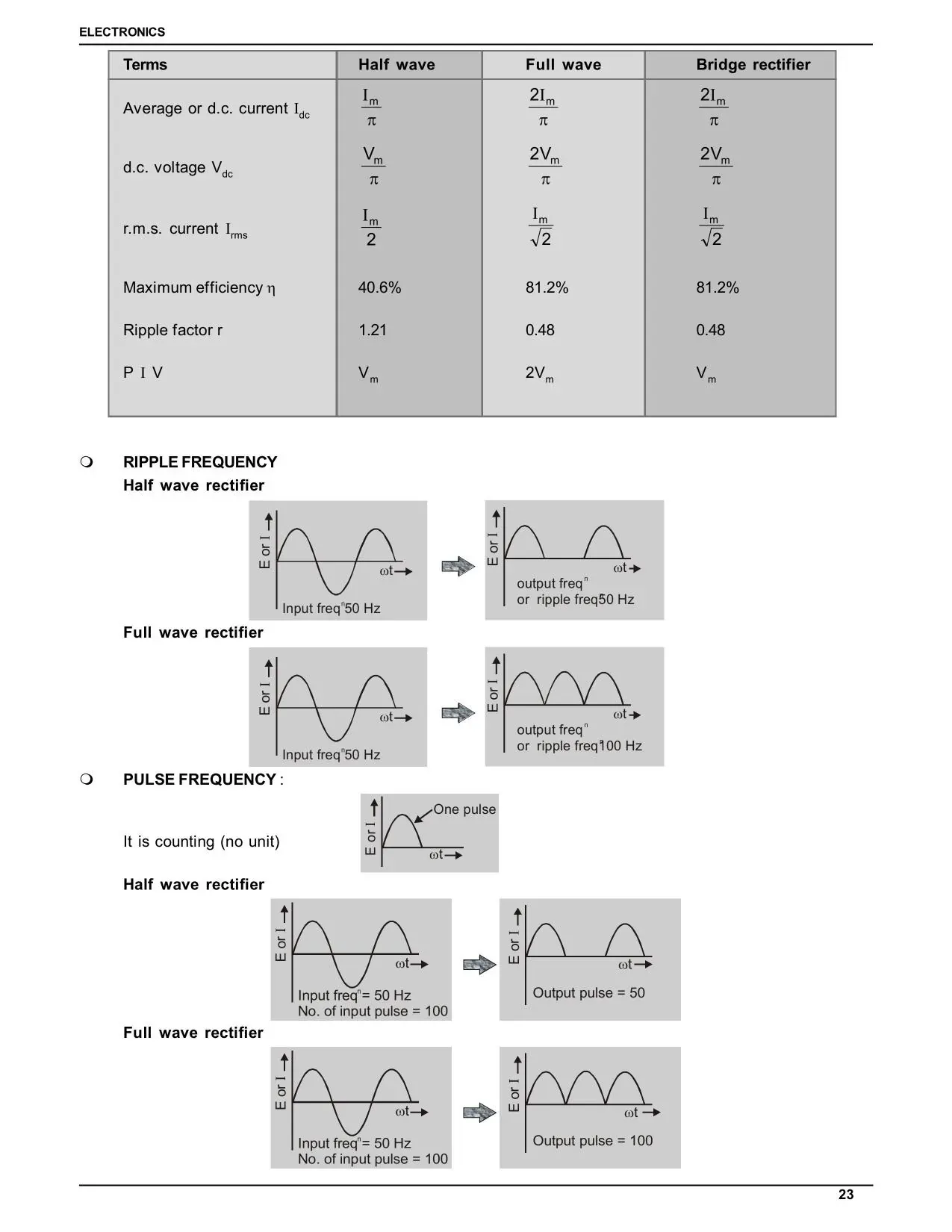
Rectifier | Diodes | Output frequency | Maximum efficiency |
|---|---|---|---|
Half-wave | 1 | $f$ | $\eta = \dfrac{4}{\pi^2} \approx 40.6\%$ |
Full-wave (centre-tap) | 2 | $2f$ | $\eta = \dfrac{8}{\pi^2} \approx 81.2\%$ |
Full-wave (bridge) | 4 | $2f$ | $\eta = \dfrac{8}{\pi^2} \approx 81.2\%$ |
For a peak current $I_m$, the average (dc) current is $I_{dc} = \dfrac{I_m}{\pi}$ for a half-wave rectifier and $I_{dc} = \dfrac{2I_m}{\pi}$ for a full-wave rectifier. The output of a rectifier is pulsating DC. A capacitor filter smooths it.
Zener Diode, LED, Photodiode and Solar Cell in Semiconductor Electronics Class 12 Notes
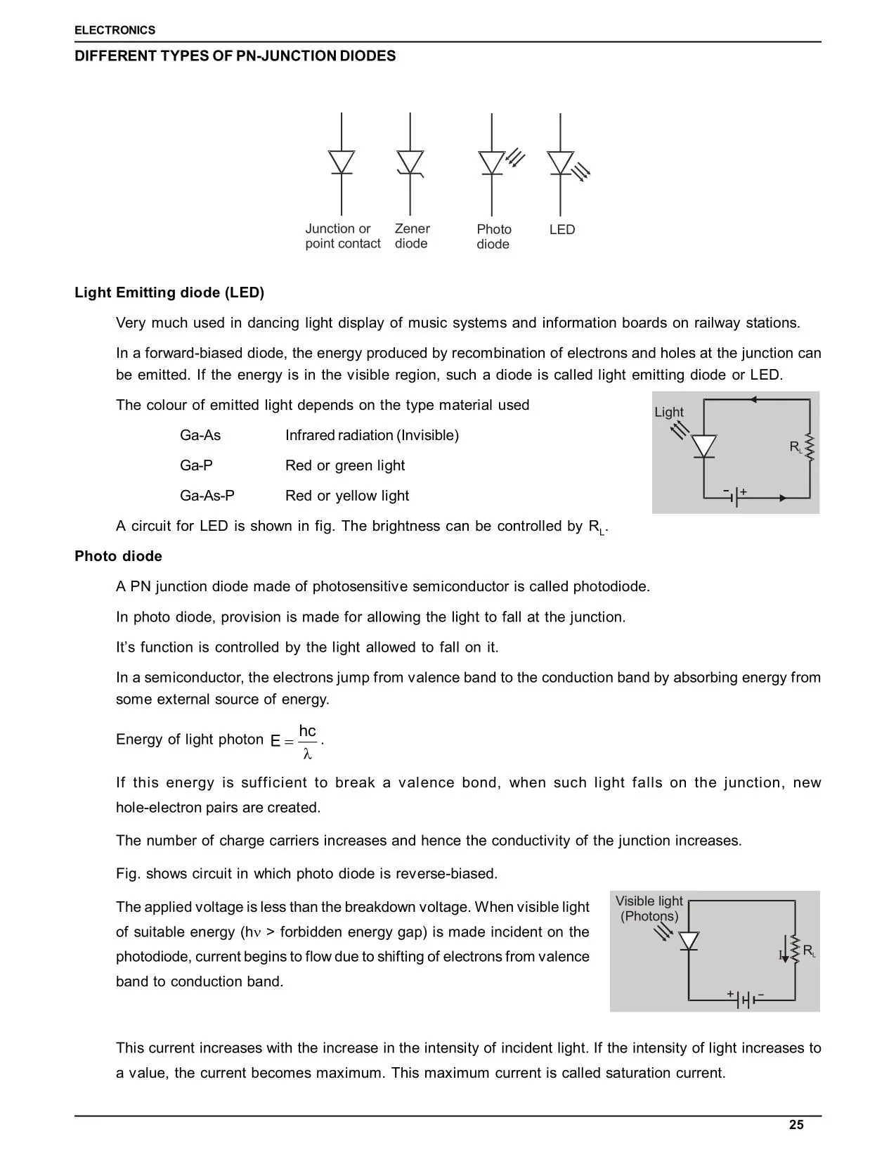
Device | Biasing | Working | Use |
|---|---|---|---|
Zener diode | Reverse bias, operated in the breakdown region | The voltage across it stays almost constant at $V_Z$ | Voltage regulator |
LED | Forward bias | Electron–hole recombination gives out photons | Indicators, displays |
Photodiode | Reverse bias | Light creates carriers, so the current rises with the light intensity | Light detectors |
Solar cell | No external bias | Photovoltaic effect: light creates a voltage | Converts light into electrical energy |
Zener regulator: the output voltage stays at $V_Z$. With a series resistor $R_s$, an input $V_{in}$, a load current $I_L$ and a Zener current $I_Z$:
$$R_s = \frac{V_{in} - V_Z}{I_Z + I_L}$$
LED colour: the photon energy is about the band gap, so
$$E = h\nu = \frac{hc}{\lambda} \approx E_g, \qquad \lambda\ (\text{in nm}) \approx \frac{1240}{E_g\ (\text{in eV})}$$
Logic Gates in Semiconductor Electronics Class 12 Notes
Logic gates work on binary inputs (0 and 1). The Boolean expression of each gate is:
Gate | Boolean expression | Output is 1 when |
|---|---|---|
AND | $Y = A \cdot B$ | Both inputs are 1 |
OR | $Y = A + B$ | At least one input is 1 |
NOT | $Y = \bar{A}$ | The input is 0 |
NAND | $Y = \overline{A \cdot B}$ | Not both inputs are 1 |
NOR | $Y = \overline{A + B}$ | Both inputs are 0 |
Truth Table
$A$ | $B$ | AND | OR | NAND | NOR |
|---|---|---|---|---|---|
0 | 0 | 0 | 0 | 1 | 1 |
0 | 1 | 0 | 1 | 1 | 0 |
1 | 0 | 0 | 1 | 1 | 0 |
1 | 1 | 1 | 1 | 0 | 0 |
For the NOT gate, an input of 0 gives 1, and an input of 1 gives 0.
Universal Gates and De Morgan’s Laws
NAND and NOR are universal gates, because every other gate can be built from only NAND gates or only NOR gates. De Morgan’s laws are used to convert between the gates:
$$\overline{A + B} = \bar{A} \cdot \bar{B}, \qquad \overline{A \cdot B} = \bar{A} + \bar{B}$$
- NOT from NAND: join both inputs of a NAND gate, so $Y = \overline{A \cdot A} = \bar{A}$.
- OR from NAND: $Y = \overline{\bar{A} \cdot \bar{B}} = A + B$, using a NAND gate on the inverted inputs.
Transistors: Extra Reading in Semiconductor Electronics Class 12 Notes
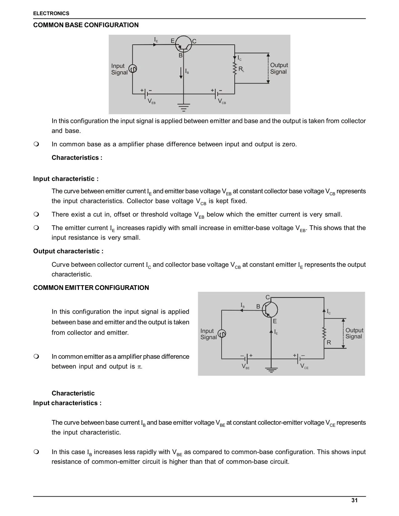
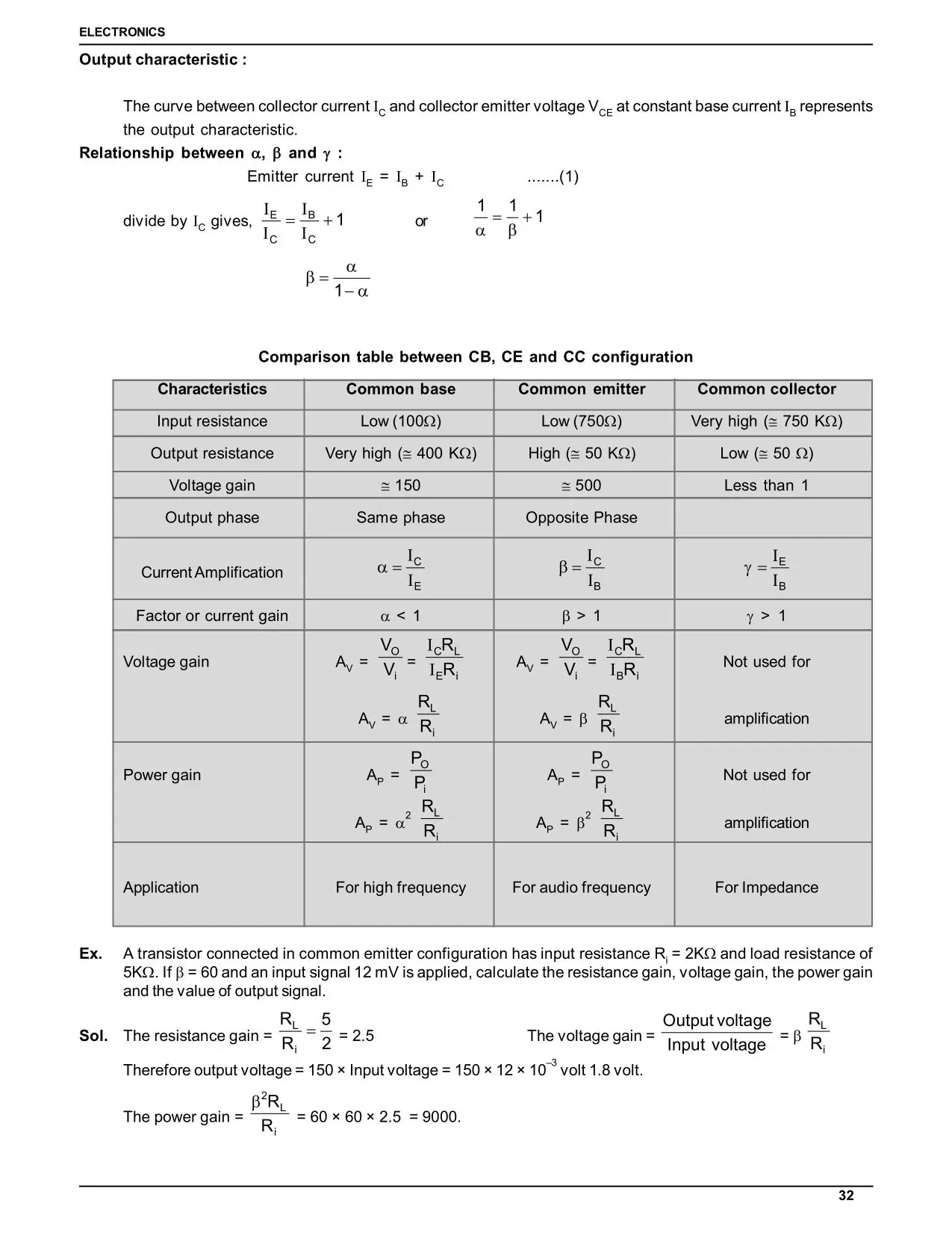
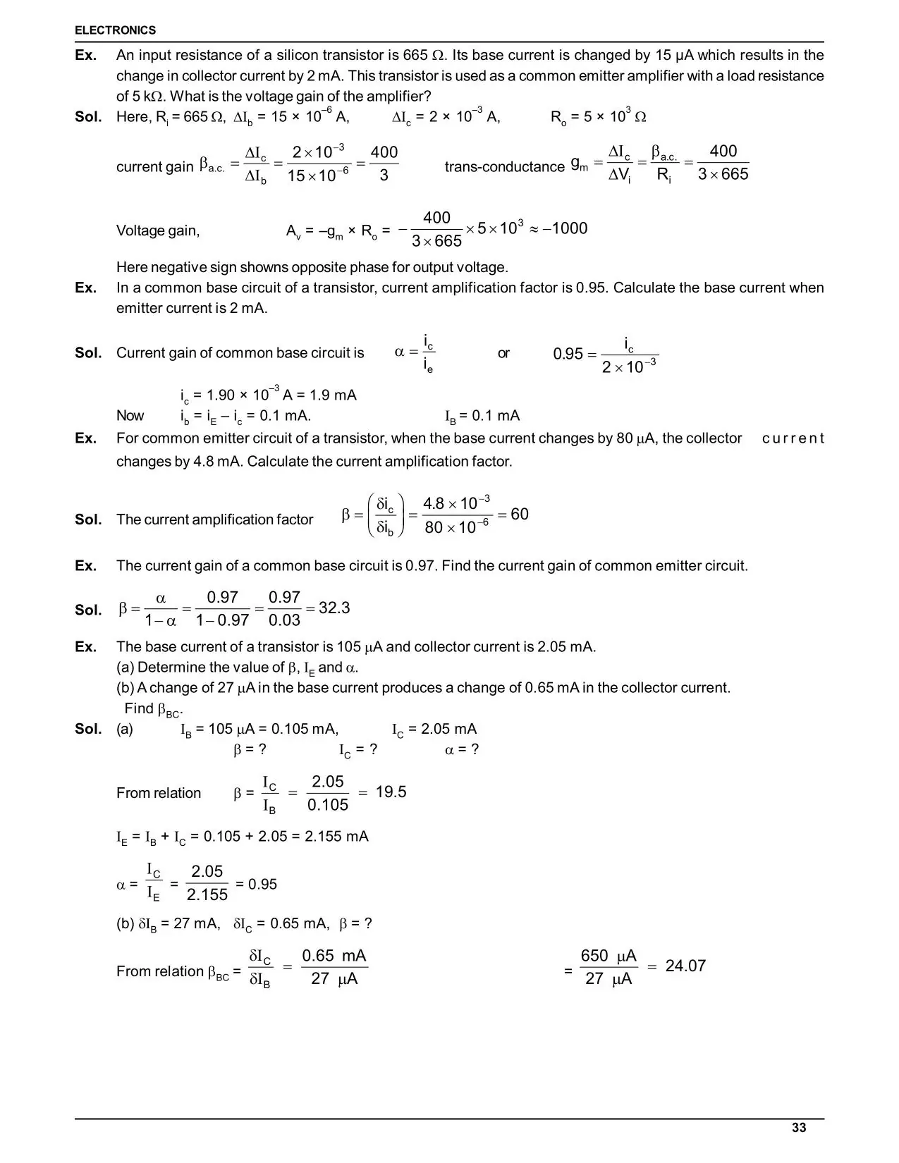
Transistors and amplifiers are not part of the CBSE 2026-27 syllabus or the JEE Main 2026 list, so treat this section as extra reading. A transistor has three regions (emitter, base and collector). The base is thin and lightly doped, and the emitter is heavily doped. The main relations are:
$$I_E = I_B + I_C, \qquad \alpha = \frac{I_C}{I_E}, \qquad \beta = \frac{I_C}{I_B}, \qquad \beta = \frac{\alpha}{1 - \alpha}$$
A transistor works as a switch: in saturation (both junctions forward biased), it is ON, and in cut-off (both junctions reverse biased), it is OFF. The XOR gate, $Y = A \oplus B = A\bar{B} + \bar{A}B$, is also outside the lists.
Key Formulas in Semiconductor Electronics Class 12 Notes
Concept | Formula |
|---|---|
Intrinsic semiconductor | $n_e = n_h = n_i$ |
Mass action law | $n_e\, n_h = n_i^{\,2}$ |
Dynamic resistance | $r_d = \dfrac{\Delta V}{\Delta I}$ |
Half-wave rectifier efficiency | $\eta_{max} = \dfrac{4}{\pi^2} \approx 40.6\%$ |
Full-wave rectifier efficiency | $\eta_{max} = \dfrac{8}{\pi^2} \approx 81.2\%$ |
Zener series resistor | $R_s = \dfrac{V_{in} - V_Z}{I_Z + I_L}$ |
LED wavelength | $\lambda\ (\text{nm}) \approx \dfrac{1240}{E_g\ (\text{eV})}$ |
NAND and NOR | $Y = \overline{A \cdot B}$ and $Y = \overline{A + B}$ |
De Morgan’s laws | $\overline{A + B} = \bar{A}\bar{B}$ and $\overline{AB} = \bar{A} + \bar{B}$ |
Solved Examples from Semiconductor Electronics Class 12 Notes
Example 1 (mass action law): In an n-type silicon sample, $n_i = 1.5 \times 10^{16}\ \text{m}^{-3}$ and $n_e = 4.5 \times 10^{22}\ \text{m}^{-3}$. Find $n_h$.
$n_h = \dfrac{n_i^{\,2}}{n_e} = \dfrac{(1.5 \times 10^{16})^2}{4.5 \times 10^{22}} = 5 \times 10^{9}\ \text{m}^{-3}$.
Example 2 (LED colour): An LED is made of a semiconductor with $E_g = 2.0$ eV. Find the wavelength of the light that it emits.
$\lambda \approx \dfrac{1240}{2.0} = 620$ nm, which is red-orange light.
Example 3 (rectifier frequency): A rectifier is fed with a 50 Hz AC supply. Find the output frequency of a half-wave and a full-wave rectifier.
The half-wave rectifier gives 50 Hz, and the full-wave rectifier gives $2 \times 50 = 100$ Hz.
Example 4 (Zener regulator): A 6 V Zener diode is connected to a 12 V supply through a series resistor. The load current is 20 mA, and the Zener must carry at least 5 mA. Find $R_s$.
$R_s = \dfrac{12 - 6}{5 \times 10^{-3} + 20 \times 10^{-3}} = \dfrac{6}{0.025} = 240\ \Omega$.
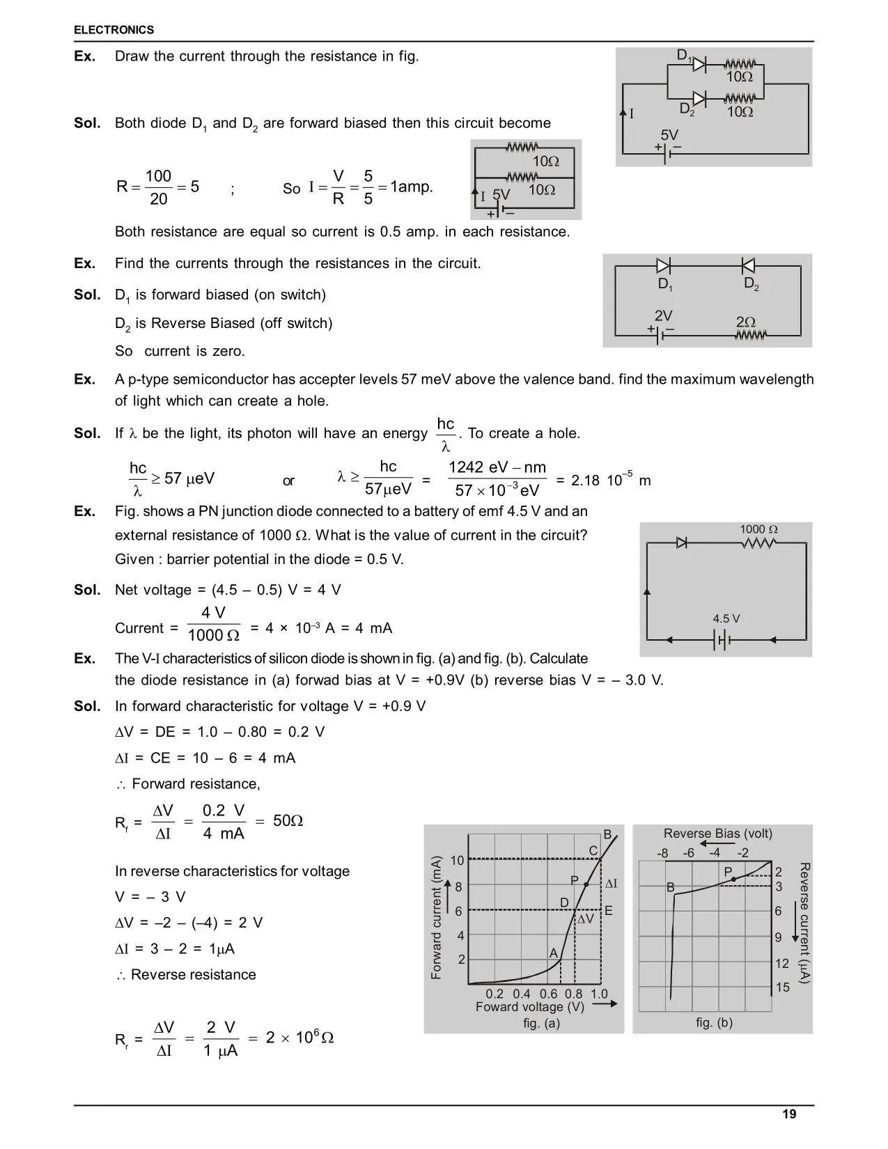
Example 5 (diode circuit): A silicon diode is forward biased in series with a 1 kΩ resistor and a 5 V battery. Find the current.
$I = \dfrac{5 - 0.7}{1000} = 4.3$ mA.
Example 6 (dynamic resistance): A change of 0.1 V across a forward-biased diode changes the current by 5 mA. Find the dynamic resistance.
$r_d = \dfrac{\Delta V}{\Delta I} = \dfrac{0.1}{5 \times 10^{-3}} = 20\ \Omega$.
Example 7 (logic gates): A NAND gate receives $\bar{A}$ and $\bar{B}$ as its inputs. What is the output in terms of $A$ and $B$?
$Y = \overline{\bar{A} \cdot \bar{B}} = A + B$ (De Morgan’s law), so the circuit works as an OR gate.
Common Mistakes in Semiconductor Electronics Class 12 Notes Problems
Mistake | Correct approach |
|---|---|
Thinking that an n-type semiconductor is negatively charged | It is neutral. Only the majority carrier is the electron. |
Saying that conductivity of a semiconductor falls with temperature | It rises, because more electron–hole pairs form |
Connecting a Zener diode in forward bias as a regulator | Operate it in reverse breakdown |
Writing the barrier potential as the supply voltage | The barrier is about 0.7 V for Si and 0.3 V for Ge. The supply is a separate voltage. |
Forgetting that a full-wave rectifier doubles the frequency | Output frequency is $2f$ |
Using the wrong output of a NAND or NOR gate | Find the AND or OR output first, and then invert it |
Studying topics outside the syllabus | Check the table at the top of this page |
How to Study Semiconductor Electronics Class 12 Notes
- Read the NCERT chapter, and mark the parts that your exam includes. Use the table at the top of this page.
- Learn the device table (biasing, working, use) and the logic gate truth tables from memory.
- Practise the numericals on rectifiers, Zener regulators and diode circuits, and then the Boolean problems with De Morgan’s laws.
- Revise with eSaral’s Class 12 Physics revision notes (Chapter 14 PDF) and the JEE Main Physics revision notes (Unit 19). For fast formula revision, use eSaral’s free Physics revision series on YouTube. Then practise with eSaral’s NEET chapter-wise PYQs and JEE Main chapter-wise PYQs.
Frequently Asked Questions
What is the difference between a conductor, a semiconductor and an insulator in Class 12?
The difference is the band gap. In a conductor, the bands overlap, so electrons move freely. A semiconductor has a small gap (below about 3 eV), so some electrons cross it at room temperature. An insulator has a large gap (above about 3 eV), so almost no electron crosses it. These Semiconductor Electronics Class 12 Notes on eSaral explain this with the energy band diagram.
What are intrinsic and extrinsic semiconductors?
In Semiconductor Electronics Class 12 Notes, an intrinsic semiconductor is pure silicon or germanium, with $n_e = n_h = n_i$. An extrinsic semiconductor is doped. A pentavalent dopant makes an n-type semiconductor with electrons as majority carriers, and a trivalent dopant makes a p-type semiconductor with holes as majority carriers. Both types are electrically neutral.
What happens at a p-n junction, and why does a depletion layer form?
In Semiconductor Electronics Class 12 Notes, electrons diffuse from the n-side to the p-side, and holes diffuse the other way. They recombine near the junction, which leaves behind fixed ions and forms a depletion layer with no mobile carriers. The layer creates a barrier potential that stops further diffusion.
What is the difference between forward bias and reverse bias?
In forward bias, the p-side is joined to the positive terminal, the barrier shrinks, and the current rises sharply after the knee voltage. In reverse bias, the barrier grows, the depletion layer widens, and only a very small reverse saturation current flows. This is the basis of the diode as a rectifier in Semiconductor Electronics Class 12 notes.
Are transistors in the JEE Main 2026 syllabus?
No. In Semiconductor Electronics Class 12 Notes, the point is clear: Unit 19 of the JEE Main 2026 syllabus lists semiconductors, the diode, the rectifier, the LED, the photodiode, the solar cell, the Zener diode as a voltage regulator and the logic gates OR, AND, NOT, NAND and NOR. Transistors and amplifiers are not listed, and they were also removed from the CBSE syllabus. Check the NMC syllabus for NEET.
Which Semiconductor Electronics topics are in the CBSE Class 12 syllabus?
The Electronic Devices unit carries 7 marks. It includes qualitative ideas of energy bands, and the semiconductor diode with its I–V characteristics in forward and reverse bias and its use as a rectifier. The LED, photodiode, solar cell, Zener diode and logic gates were removed from the CBSE syllabus, so check the latest CBSE syllabus. These Semiconductor Electronics Class 12 Notes mark each topic.
Why are NAND and NOR called universal gates?
In Semiconductor Electronics Class 12 Notes, every other logic gate can be built using only NAND gates or only NOR gates. For example, joining both inputs of a NAND gate gives a NOT gate, and a NAND gate on two inverted inputs gives an OR gate, as De Morgan’s law shows.
Which chapter number is Semiconductor Electronics in Class 12 Physics?
In the NCERT Class 12 Physics book, Semiconductor Electronics: Materials, Devices and Simple Circuits is Chapter 14, the last chapter. These Semiconductor Electronics Class 12 Notes follow the chapter name.
Where can I find more Class 12 Physics notes on eSaral?
eSaral has chapter-wise Class 12 Physics revision notes, handwritten notes, NCERT solutions and a free Physics revision series on YouTube, linked with these Semiconductor Electronics Class 12 Notes on this page.
Team eSaral
eSaral Academic and Editorial Team
Team eSaral is the collective author profile for educational content created by eSaral’s teachers and academic contributors. The team draws on expertise from IIT graduates, doctors, experienced educators and subject specialists to develop resources for JEE, NEET and school students. Our articles aim to explain concepts clearly and help students study with confidence.
Related Posts

BITSAT 2027: Registration Date, Exam Date, Syllabus, Eligibility, Pattern & Fees
BITSAT 2027 exam dates, registration timeline, eligibility criteria, exam pattern, marking scheme, syllabus and fees in one page.
BITSAT Previous Year Question Paper PDF (2017-2026)
Download BITSAT previous year question papers PDF from 2017 to 2026,session-wise. Memory-based papers,exam pattern, paper analysis and how to practise
CBSE Class 10 Date Sheet 2027: Expected Exam Dates, Release Date, Admit Card & Result Timeline
CBSE Class 10 date sheet 2027 is awaited. See the expected exam dates, release window, how to download the PDF, admit card and result timelines.
NCERT Physics Class 10 Book PDF in Hindi 2026-27 – भौतिक विज्ञान के 4 अध्याय (Free Download)
NCERT Physics Class 10 book PDF in Hindi 2026-27: download all 4 chapters (अध्याय 9–12) free, with topics and important formulas.

NCERT Biology Class 9 Book Anveshan PDF in Hindi - जीव विज्ञान कक्षा 9 पुस्तक अन्वेषण PDF
Download NCERT Biology Class 9 book PDF in Hindi chapterwise for 2026-27: Cell, Tissues, Reproduction and Diversity. Free PDFs.

Essay On Artificial Intelligence in English (100,150, 200, 250, 300, 500 Words)
This is in contrast to the natural intelligence of humans. With Artificial Intelligence, machines can perform

Essay on 78th India Independence Day in English for Student (100, 150, 200, 250, 300, 500 Words)
Read the best essays on India's Independence Day in English. Short & long essays (100, 150, 200, 250, 300, 500 words) perfect for school exams
NCERT Class 11 English Snapshots book - Free PDF download- Esaral
Download NCERT Class 11 English Snapshots book PDF for free. Get all 8 chapters, chapter-wise. Start your prep today!
NCERT Class 10 biology book pdf - Free PDF Download - eSaral
NCERT Class 10 Biology book PDF 2026-27: all 5 chapters (Life Processes to Our Environment) in English & Hindi, with CBSE syllabus, marks & practical

Essay on Global Warming in English (100,150, 200, 250, 300, 500 Words)
Global warming means the Earth is getting hotter. This happens because of things like pollution from cars and factories.