
Semiconductors - NEET Previous Year Questions with Complete Solutions
eSaral › NEET › Semiconductors - NEET Previous Year Questions with Complete Solutions

Why Semiconductors Is a Top-Scoring Physics Chapter in NEET
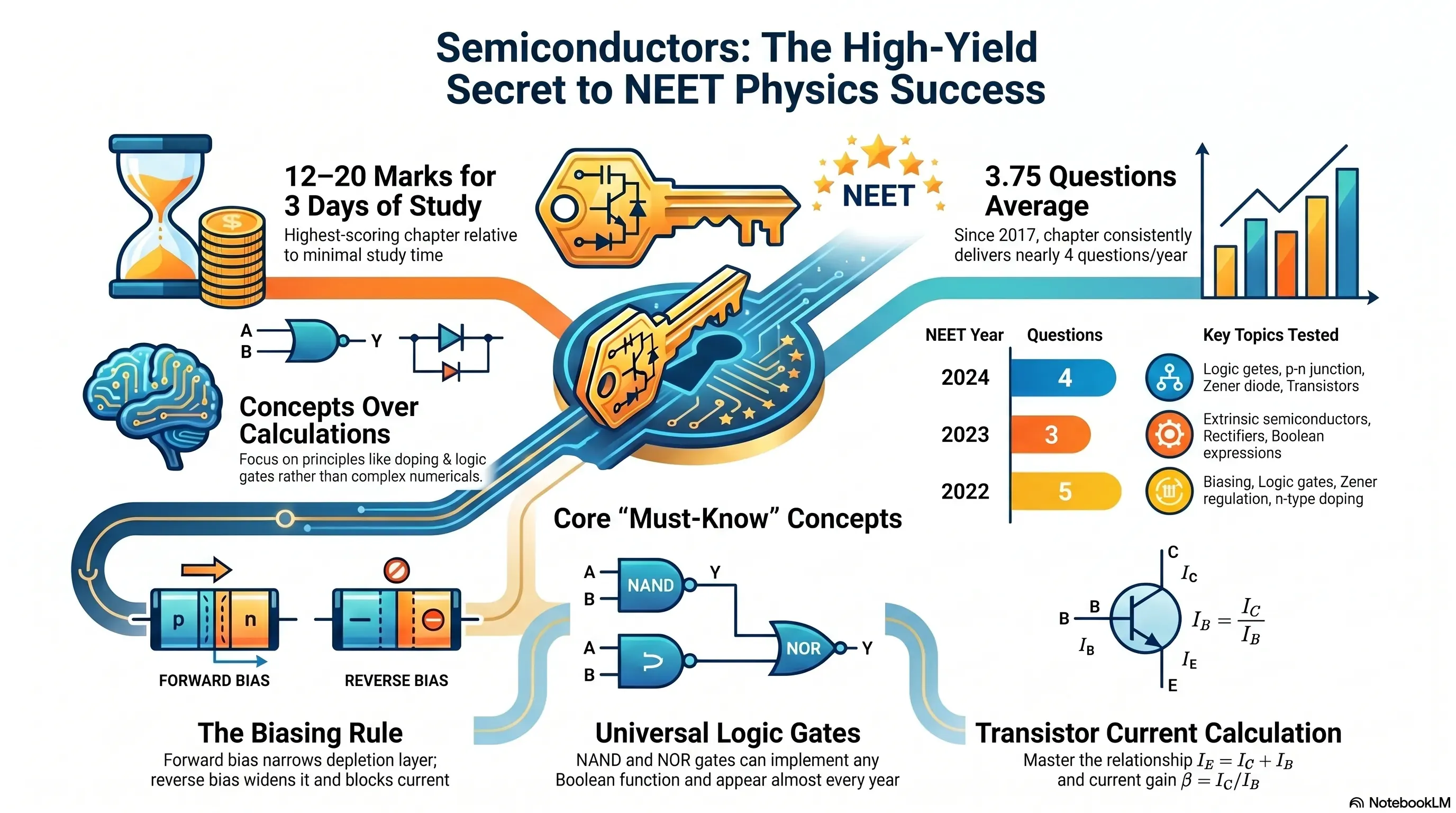
Among all Physics chapters in NEET UG, Semiconductor Electronics (Class 12, Chapter 14) is consistently one of the highest-scoring chapters — contributing 3–5 questions every year, worth approximately 12–20 marks.
What makes this chapter exceptionally valuable for NEET preparation is its nature: the questions are predominantly concept-based and fact-driven rather than mathematically intensive. Unlike chapters such as Alternating Current or Ray Optics that demand heavy numerical calculations, Semiconductors rewards students who understand the underlying principles — p-type vs n-type doping, forward vs reverse bias behaviour, rectifier circuits, and Boolean logic gates.
A student who has genuinely understood the six core concept areas in this chapter will answer every Semiconductors question in NEET correctly — because NTA recycles the same conceptual frameworks year after year with only surface-level variations.
💡 Expert Tip by eSaral Physics Faculty: "Semiconductors is the most underestimated chapter in NEET Physics. Most students think it is boring and skip deep understanding — then lose 3–4 questions on topics they could have mastered in two days. Logic gates alone contribute 1–2 questions in most years. If you can fill a truth table for AND, OR, NAND, NOR, and NOT in under 2 minutes, those are essentially free marks. Invest two days in this chapter and collect 12–20 marks reliably."
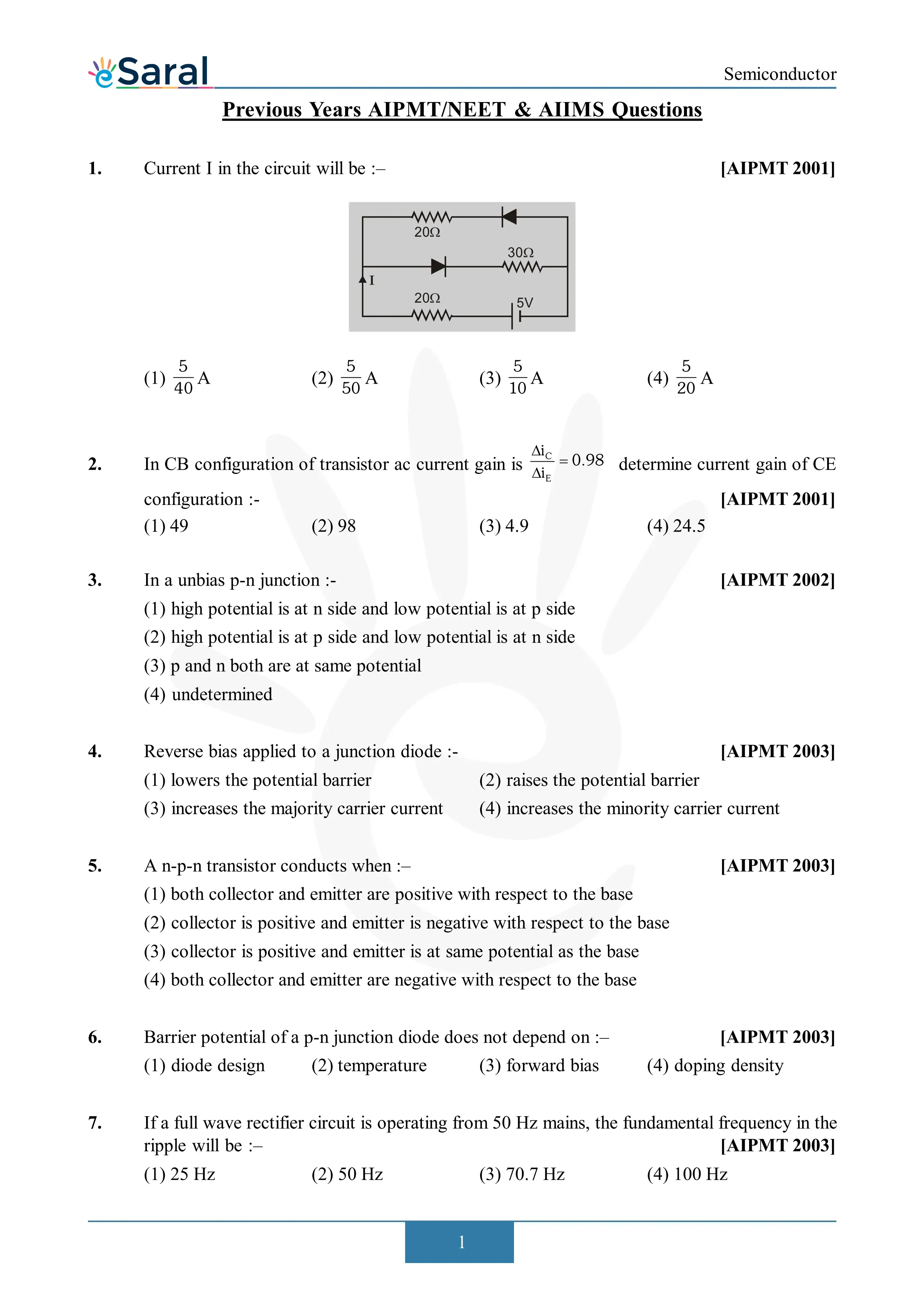
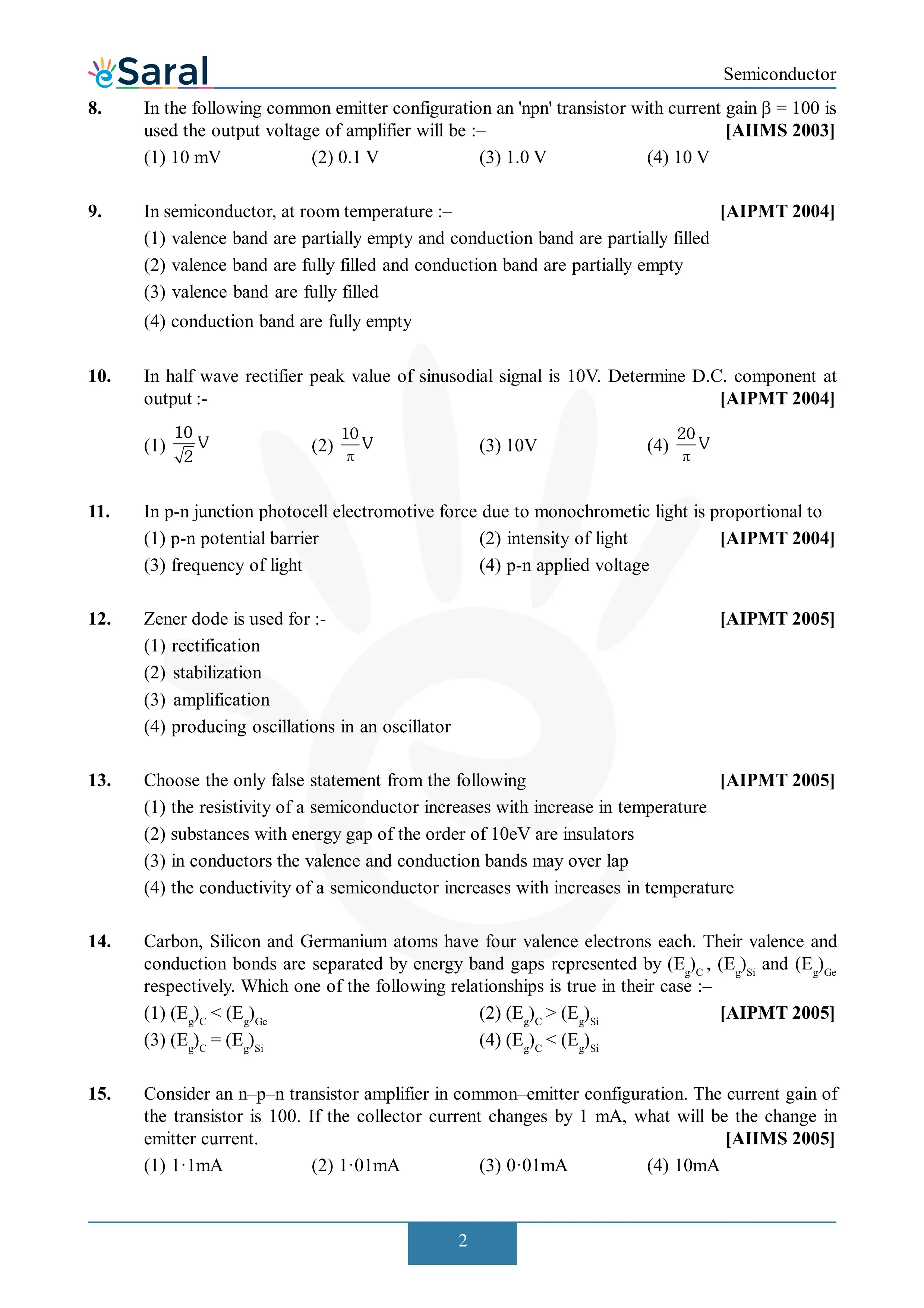
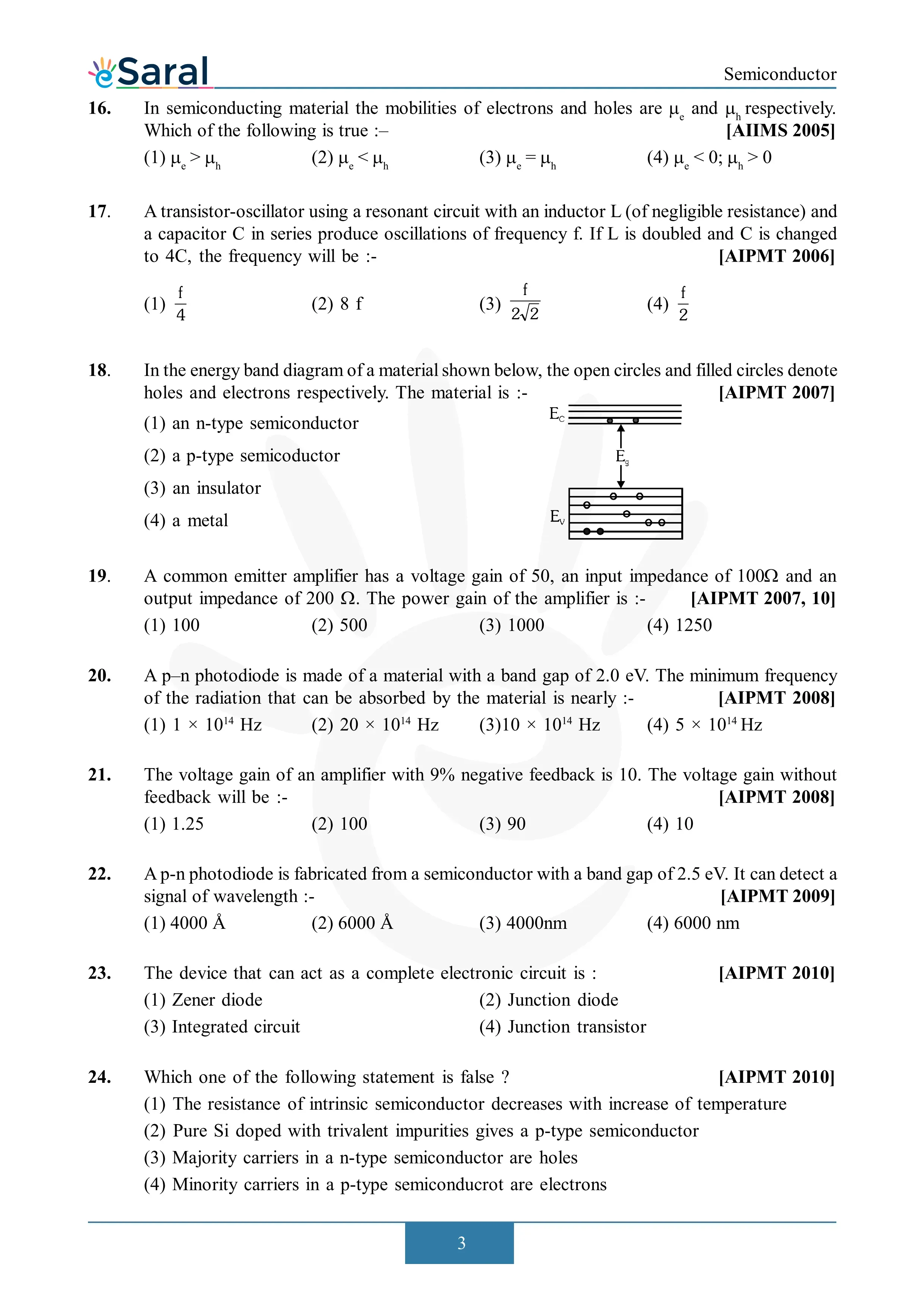
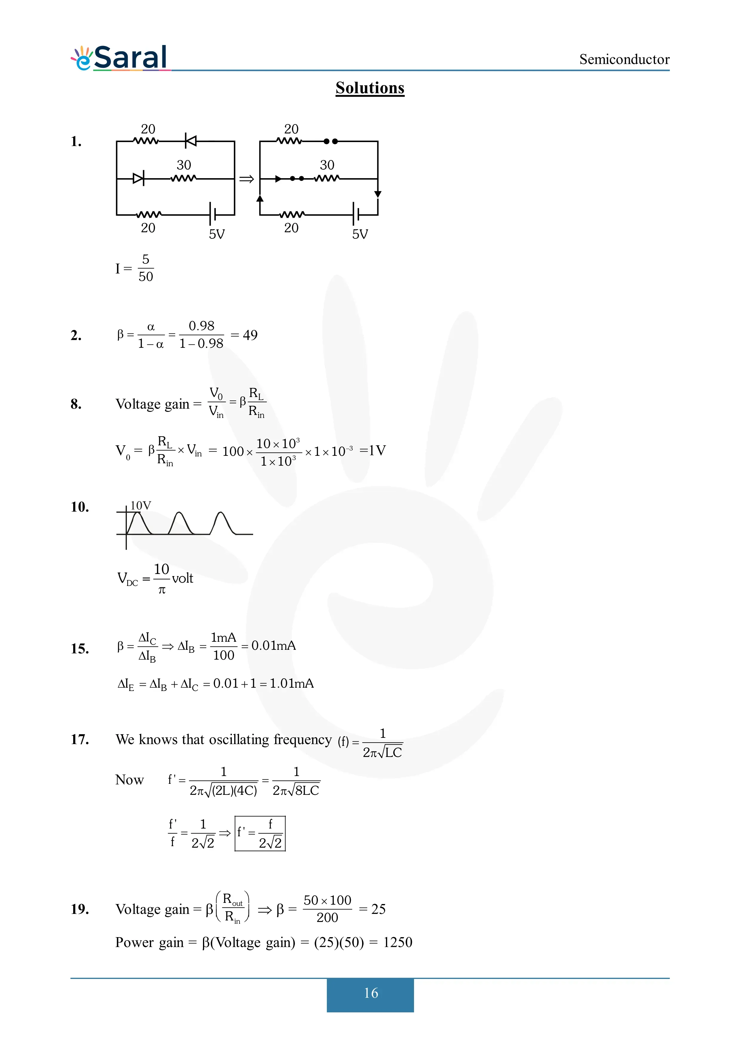
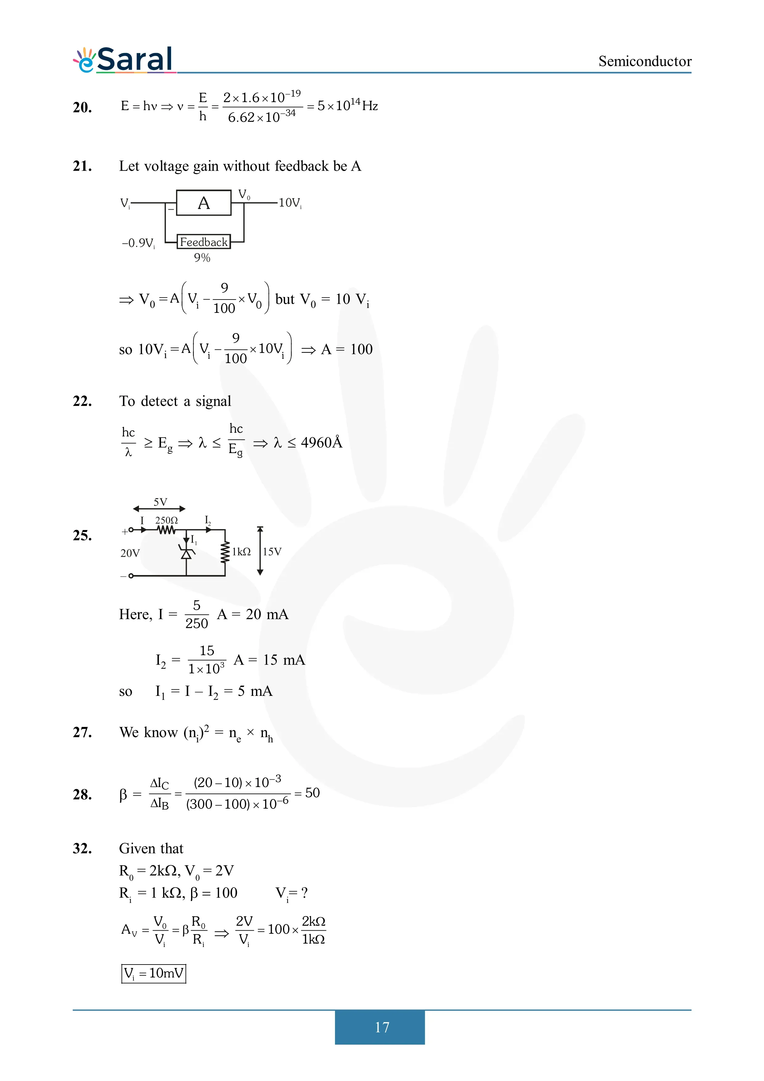
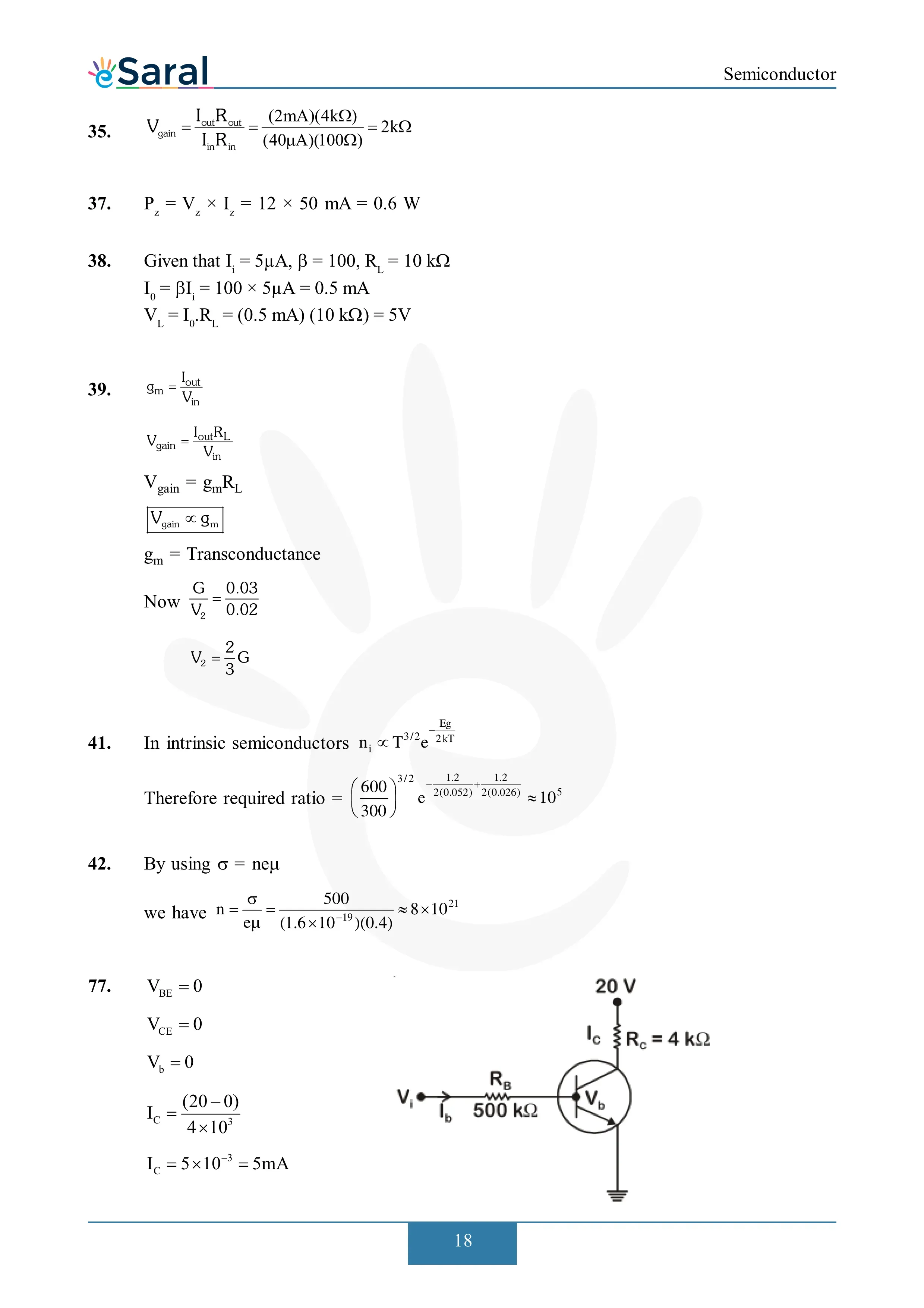
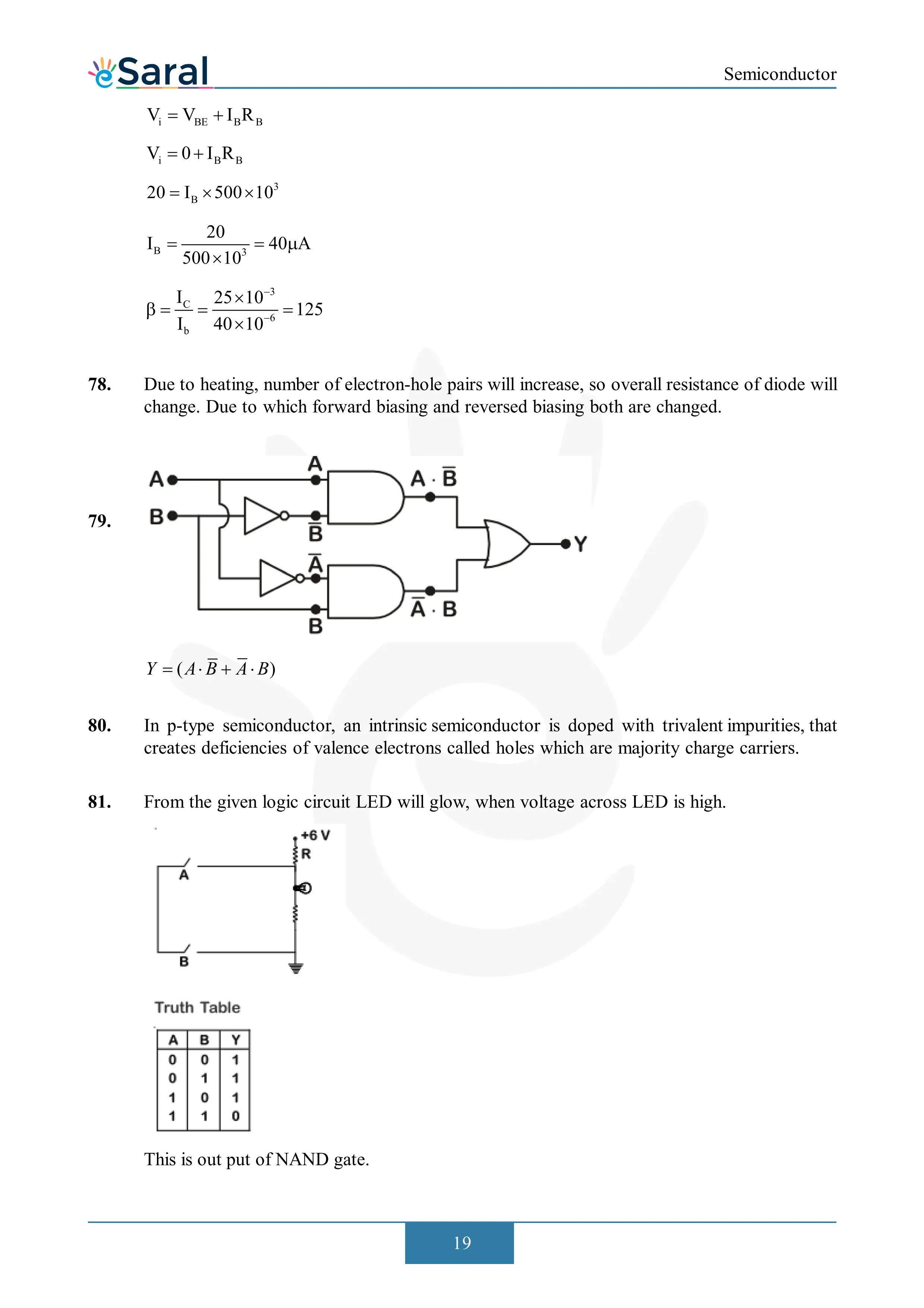
NEET Previous Year Questions — Semiconductors with Solutions
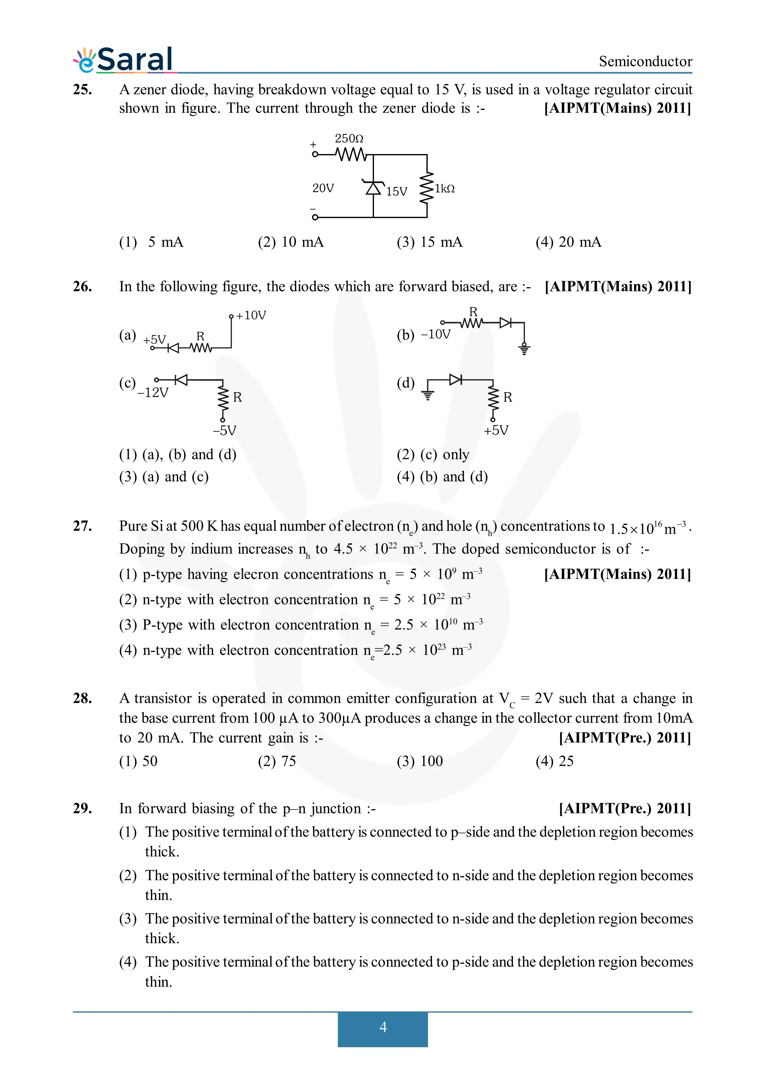
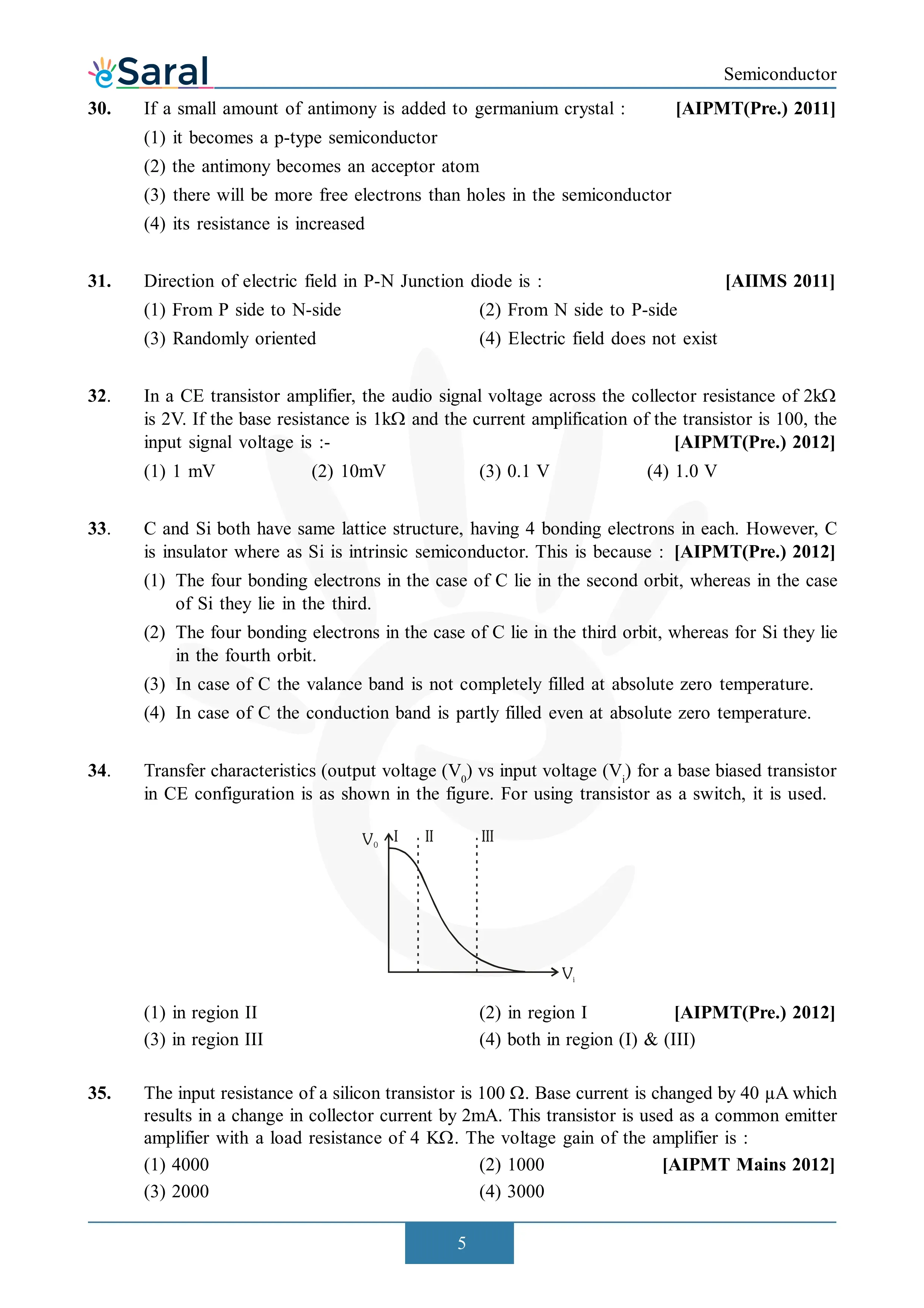
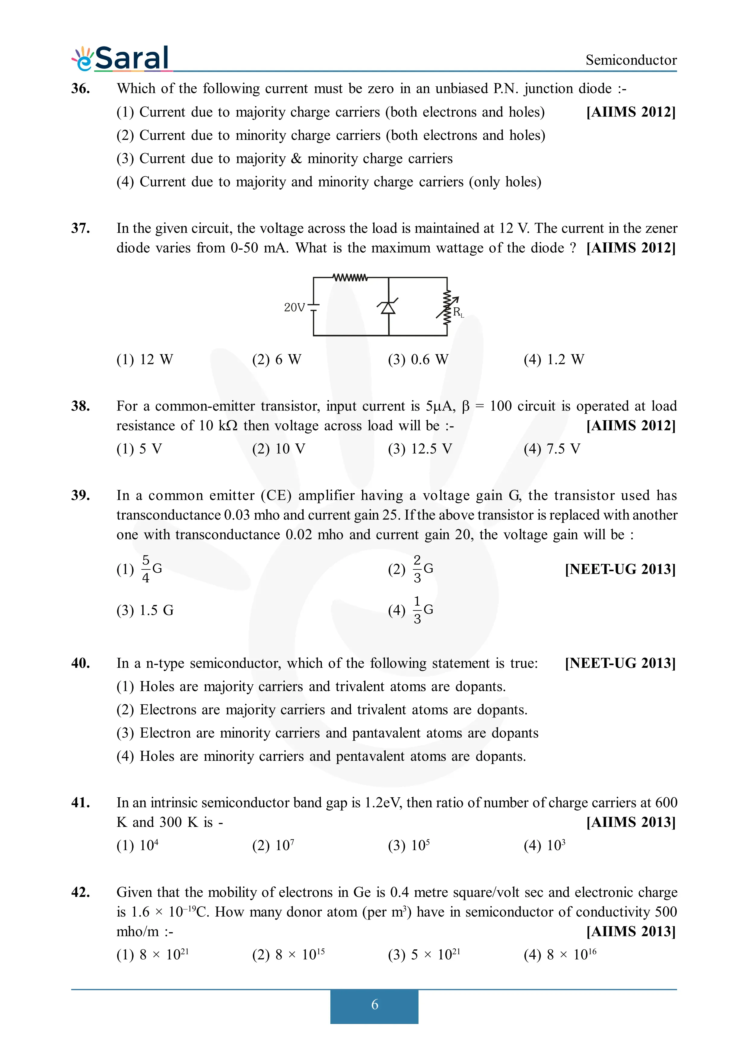
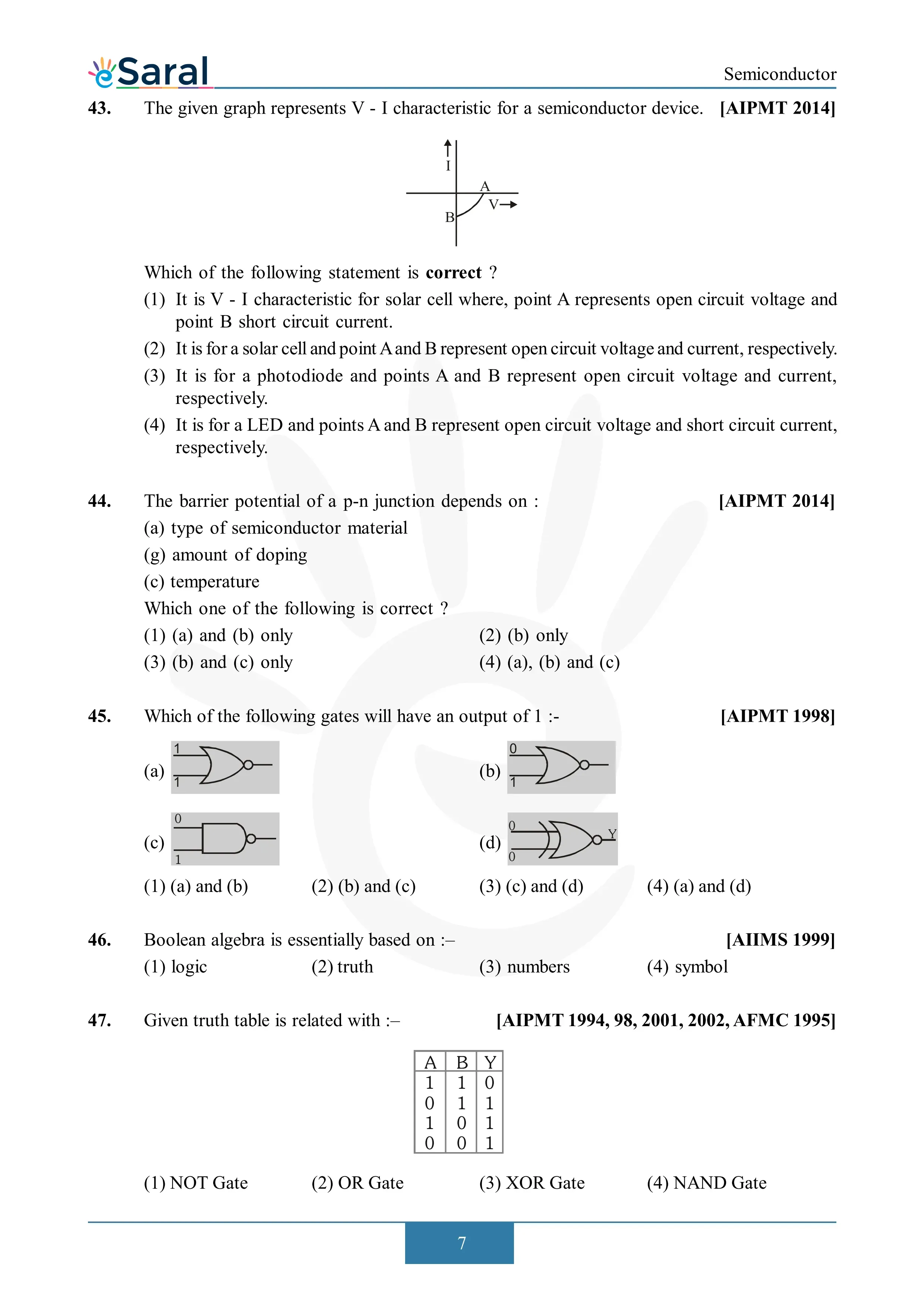
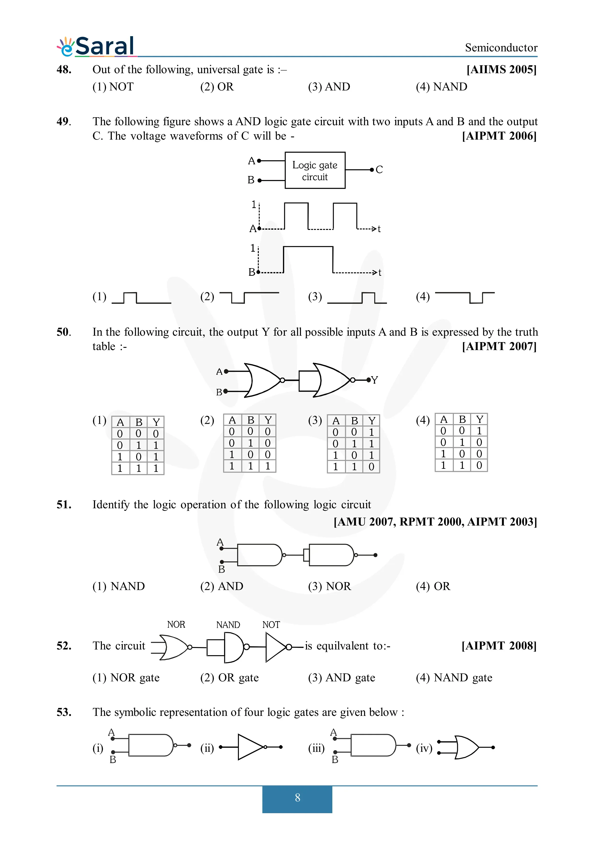
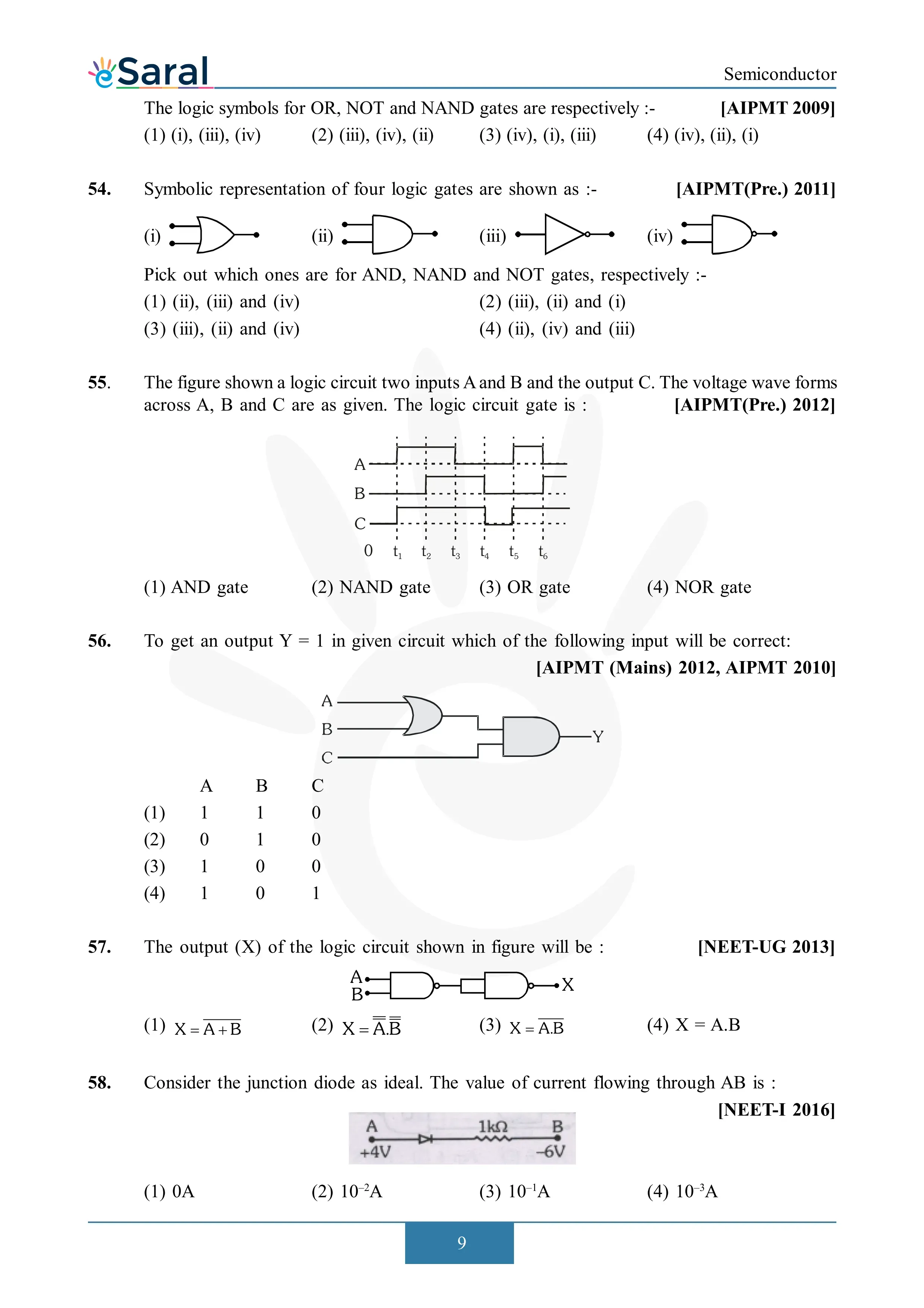
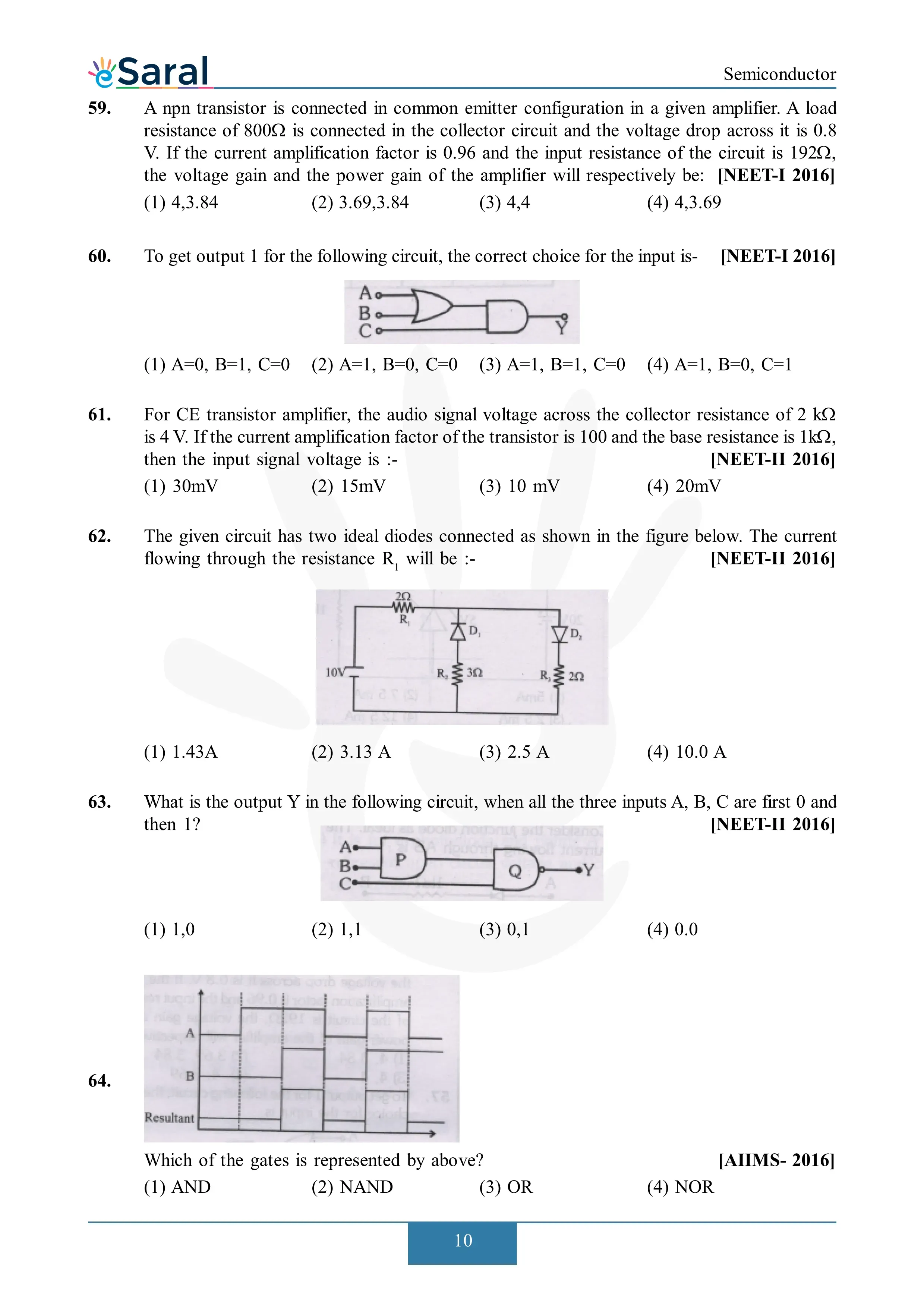
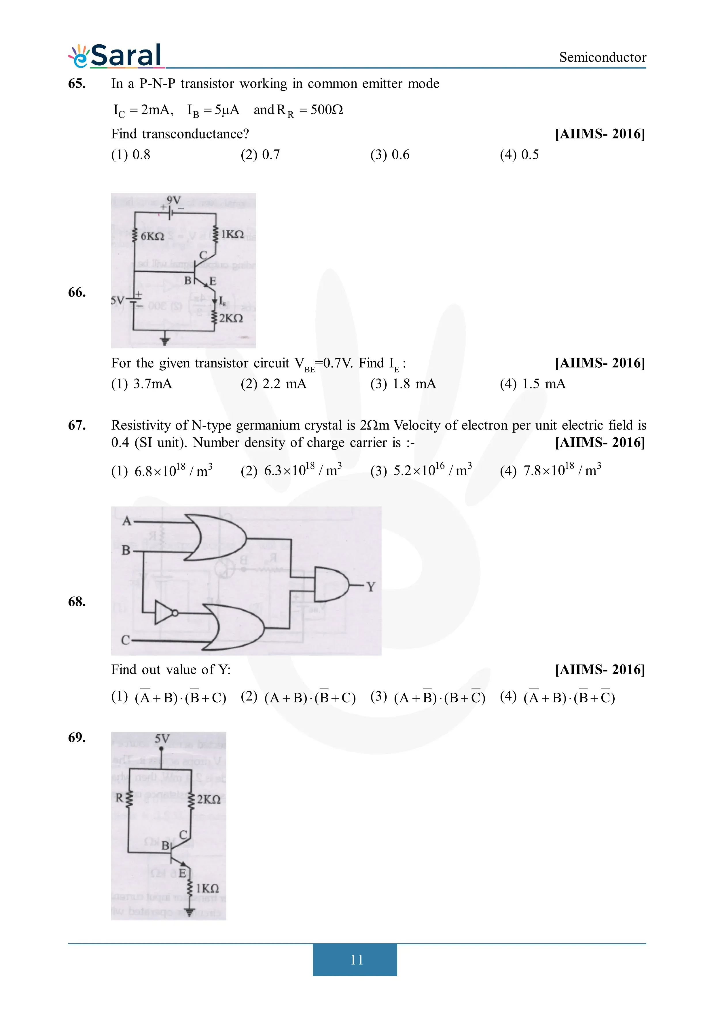
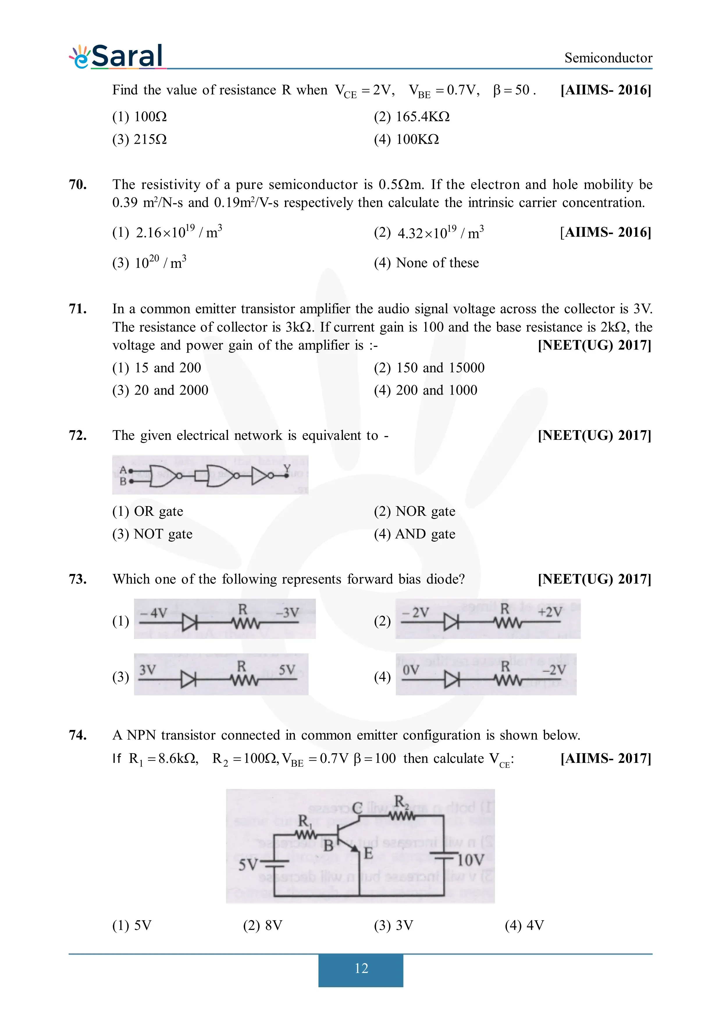
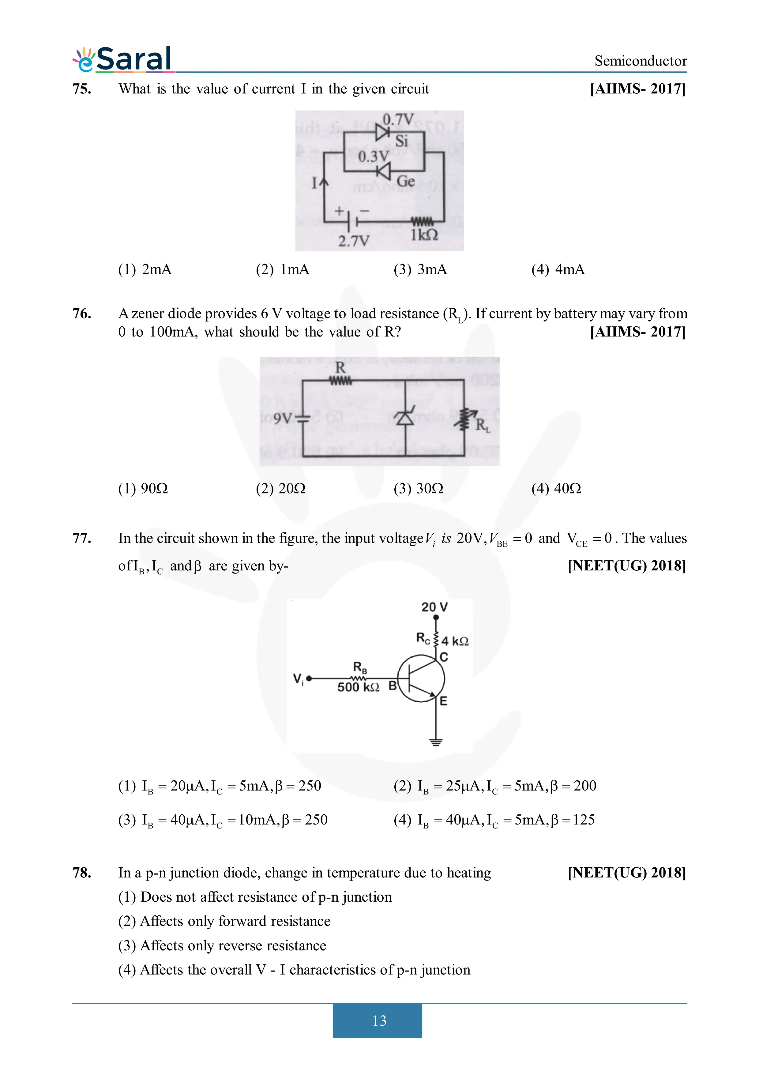
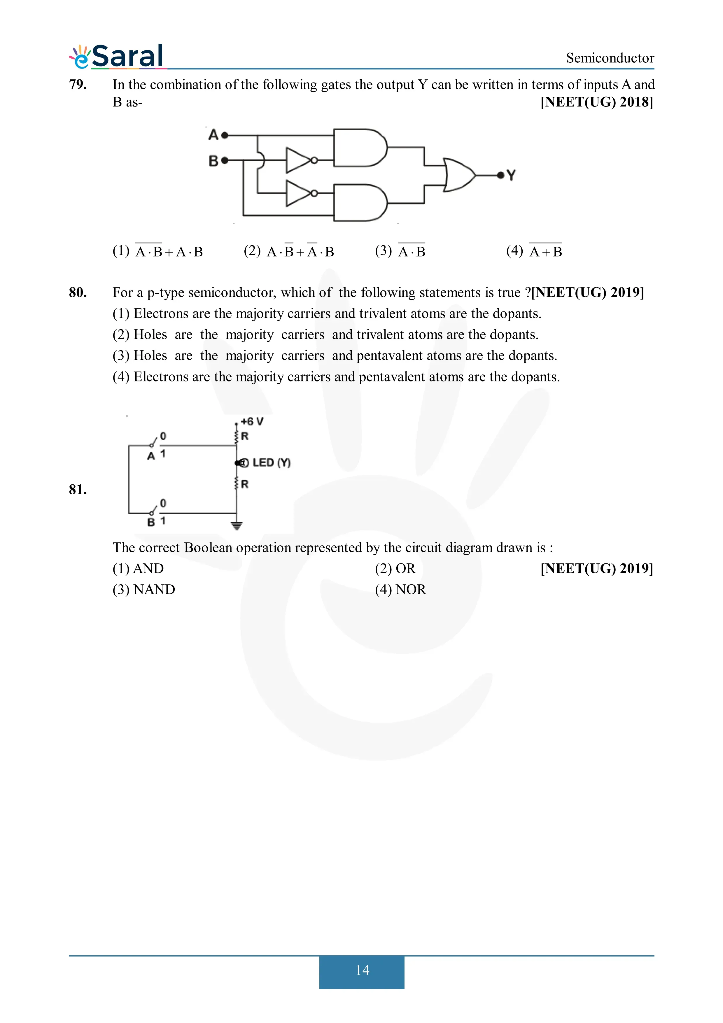
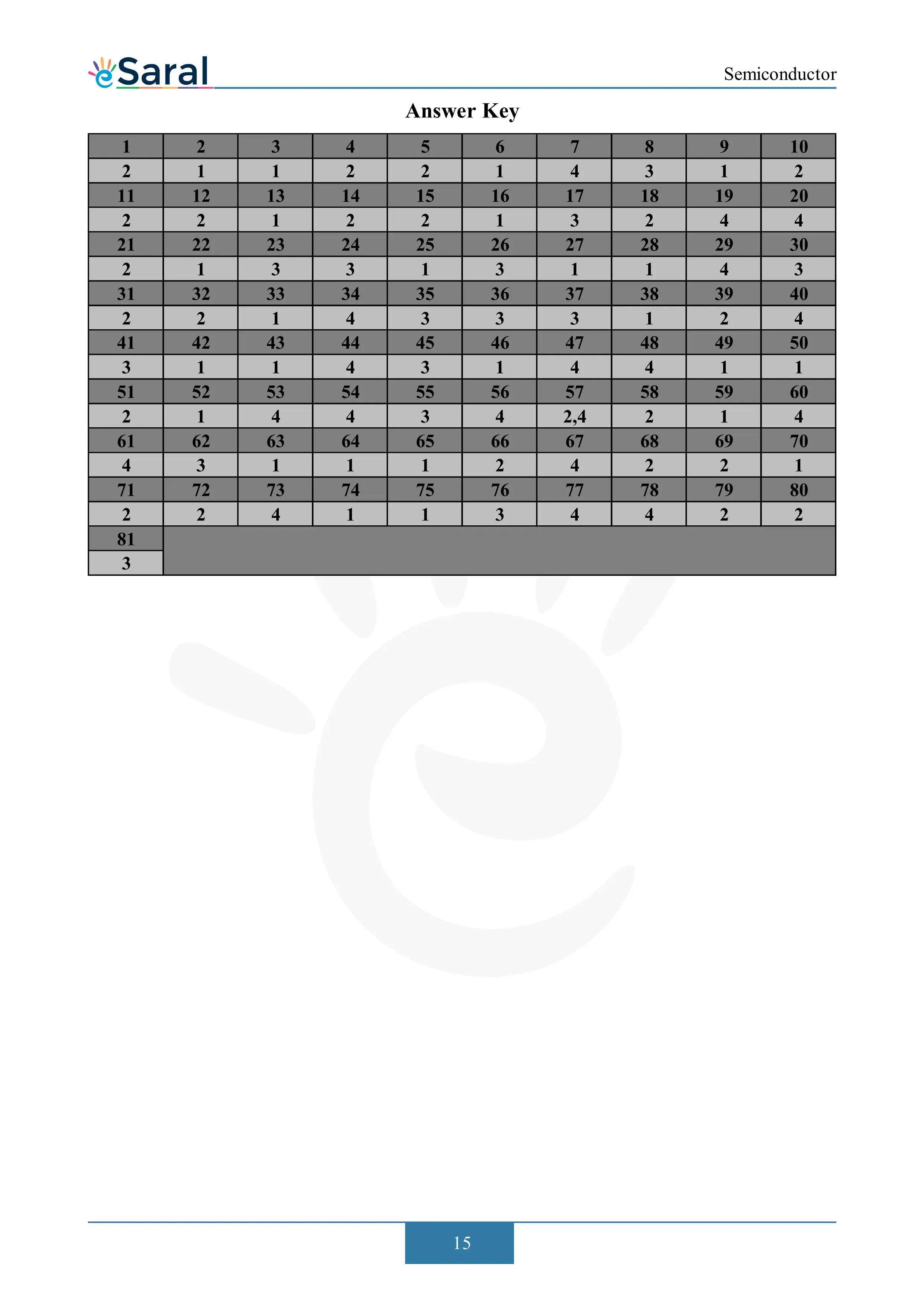
Chapter Overview: Topics and Subtopics
What This Chapter Covers
Topic | Key Subtopics | NEET Frequency |
|---|---|---|
Energy Bands | Conductor, semiconductor, insulator — band gap comparison | Medium |
Intrinsic Semiconductors | Pure Si and Ge, electron-hole pairs, thermal generation | High |
Extrinsic Semiconductors | n-type (pentavalent dopant), p-type (trivalent dopant), majority/minority carriers | Very High |
p-n Junction Formation | Depletion layer, potential barrier, contact potential | High |
p-n Junction — Forward Bias | Current flow, narrow depletion layer, low resistance | Very High |
p-n Junction — Reverse Bias | Negligible current, wide depletion layer, high resistance, breakdown | Very High |
Diode as Rectifier | Half-wave rectifier, full-wave rectifier (centre-tap and bridge), filtering | Very High |
Zener Diode | Zener breakdown, voltage regulation, reverse bias operation | Very High |
Photodiode | Reverse-biased operation, photodetection | Medium |
LED (Light Emitting Diode) | Forward bias, photon emission, energy gap and wavelength | Medium |
Solar Cell | Photovoltaic effect, no external bias | Medium |
Transistor | n-p-n and p-n-p types, emitter/base/collector, CE configuration | Very High |
Transistor as Amplifier | CE configuration, current gain (β), voltage gain | High |
Transistor as Switch | Saturation and cut-off modes | High |
Logic Gates | AND, OR, NOT, NAND, NOR — symbols, truth tables, Boolean expressions | Very High |
Universal Gates | NAND and NOR as universal gates | High |
NEET Weightage Analysis: Year-Wise Question Count
How Many Questions Come From Semiconductors in NEET?
NEET Year | Questions | Key Topics Tested |
|---|---|---|
NEET 2024 | 4 | Logic gates (NAND), p-n junction bias, Zener diode, transistor CE |
NEET 2023 | 3 | Extrinsic semiconductors, rectifier, Boolean expression |
NEET 2022 | 5 | Forward/reverse bias, logic gates (NOR), Zener regulation, n-type doping |
NEET 2021 | 4 | Transistor switch, LED, p-n junction formation, truth table |
NEET 2020 | 3 | Half-wave rectifier, depletion layer, NAND gate |
NEET 2019 | 4 | Energy bands, Zener diode, transistor amplifier, logic gates |
NEET 2018 | 3 | p-type vs n-type, full-wave rectifier, NOT gate |
NEET 2017 | 4 | p-n junction bias, transistor CE, AND/OR gates, Zener |
Average: 3.75 questions per year — approximately 15 marks. Semiconductors is the single highest-scoring Physics chapter in NEET when measured against study time required. Three days of focused preparation routinely delivers 12–20 marks.
💡 Expert Tip by eSaral Physics Faculty: "Two facts that NEET tests every single year from Semiconductors: (1) In a p-n junction, forward bias reduces the depletion layer width and allows current to flow; reverse bias increases the depletion layer width and blocks current. (2) NAND and NOR are universal gates — any logic circuit can be built using only NAND gates or only NOR gates. These two facts alone have appeared in over 14 NEET papers in the last 8 years."
Key Concepts You Must Know Before Solving PYQs
1. Intrinsic vs Extrinsic Semiconductors
Type | Definition | Charge Carriers | Example |
|---|---|---|---|
Intrinsic | Pure semiconductor; no dopants added | Electron-hole pairs (equal numbers) | Pure Si, pure Ge |
n-type | Doped with pentavalent (Group 15) atoms | Majority: electrons; Minority: holes | Si + P, As, Sb (phosphorus, arsenic, antimony) |
p-type | Doped with trivalent (Group 13) atoms | Majority: holes; Minority: electrons | Si + B, Al, In (boron, aluminium, indium) |
Critical NEET facts:
- In n-type: pentavalent dopant donates one extra electron → free electron (donor atom)
- In p-type: trivalent dopant creates one hole (acceptor atom)
- In both types: the material remains electrically neutral overall — doping does not add net charge
2. p-n Junction — Forward and Reverse Bias
Condition | Battery Connection | Depletion Layer | Current | Resistance |
|---|---|---|---|---|
No bias | None | Moderate width | Zero | — |
Forward bias | +ve terminal to p-side, −ve to n-side | Narrows | Flows (mA range) | Low |
Reverse bias | +ve terminal to n-side, −ve to p-side | Widens | Negligible (μA) | Very high |
Breakdown | Reverse bias exceeds breakdown voltage | Collapses | Large reverse current | — |
Threshold voltage (cut-in voltage):
- Germanium diode: ~0.3 V
- Silicon diode: ~0.7 V
3. Rectifiers — Half-Wave and Full-Wave
Type | Diodes Used | Output | Efficiency | Ripple |
|---|---|---|---|---|
Half-wave rectifier | 1 diode | Only positive half of AC cycle | ~40.6% | High |
Full-wave (centre-tap) | 2 diodes + centre-tap transformer | Both halves of AC cycle | ~81.2% | Lower |
Full-wave bridge | 4 diodes | Both halves of AC cycle | ~81.2% | Lower |
Key fact: A filter capacitor connected in parallel with the load reduces ripple in the output, making it closer to pure DC.
4. Zener Diode
- Operates in reverse bias — unlike a normal diode which is destroyed at breakdown
- Designed to operate at a specific Zener breakdown voltage (Vz)
- Used as a voltage regulator — maintains constant output voltage despite fluctuations in input voltage or load current
- Connected in reverse bias with a series resistor
NEET question pattern: Given a circuit with a Zener diode, find the current through the Zener or the voltage across the load. Key: voltage across load = Vz (Zener voltage) as long as the input voltage is above Vz.
5. Transistor — Key Facts for NEET
Parameter | Description |
|---|---|
Types | n-p-n (most commonly tested) and p-n-p |
Regions | Emitter (heavily doped), Base (thin, lightly doped), Collector (moderately doped, largest) |
Configurations | Common Emitter (CE), Common Base (CB), Common Collector (CC) |
CE current gain (β) | β = I_C / I_B (ratio of collector current to base current) |
Relation | I_E = I_C + I_B |
CE as amplifier | Input at base, output at collector; phase reversal of 180° |
CE as switch | Saturation = ON (both junctions forward biased); Cut-off = OFF (both junctions reverse biased) |
NEET calculation pattern: Given β and I_B, find I_C = β × I_B, then I_E = I_C + I_B.
6. Logic Gates — Truth Tables (Most Tested in NEET)
AND Gate (Output HIGH only when ALL inputs are HIGH):
A | B | Y = A·B |
|---|---|---|
0 | 0 | 0 |
0 | 1 | 0 |
1 | 0 | 0 |
1 | 1 | 1 |
OR Gate (Output HIGH when ANY input is HIGH):
A | B | Y = A+B |
|---|---|---|
0 | 0 | 0 |
0 | 1 | 1 |
1 | 0 | 1 |
1 | 1 | 1 |
NOT Gate (Output is complement of input):
A | Y = Ā |
|---|---|
0 | 1 |
1 | 0 |
NAND Gate (AND + NOT — Universal Gate):
A | B | Y = (A·B)' |
|---|---|---|
0 | 0 | 1 |
0 | 1 | 1 |
1 | 0 | 1 |
1 | 1 | 0 |
NOR Gate (OR + NOT — Universal Gate):
A | B | Y = (A+B)' |
|---|---|---|
0 | 0 | 1 |
0 | 1 | 0 |
1 | 0 | 0 |
1 | 1 | 0 |
Memory rule for NAND and NOR:
- NAND: output is 0 ONLY when ALL inputs are 1 (opposite of AND)
- NOR: output is 1 ONLY when ALL inputs are 0 (opposite of OR)
- Both NAND and NOR are universal gates — any Boolean function can be implemented using only NAND or only NOR gates
How to Study Semiconductors for Maximum NEET Marks
Step-by-Step Study Plan
Step 1 — Understand energy bands and semiconductor types (Day 1) Read NCERT Chapter 14 sections on conductors, semiconductors, and insulators — the band gap comparison. Then study intrinsic vs extrinsic semiconductors. Make a clear table: pentavalent dopant → n-type → electrons as majority carriers; trivalent dopant → p-type → holes as majority carriers. This is the foundation on which all subsequent topics rest.
Step 2 — Master p-n junction behaviour in forward and reverse bias (Day 1–2) Draw the p-n junction depletion layer in three states: no bias, forward bias, reverse bias. Write what happens to the depletion layer width and current in each case. The contrast between forward bias (narrow depletion layer, large current, low resistance) and reverse bias (wide depletion layer, negligible current, high resistance) is the single most tested concept in this chapter.
Step 3 — Study rectifier circuits with diagrams (Day 2) Draw the half-wave rectifier circuit (1 diode) and the full-wave bridge rectifier circuit (4 diodes). For each, draw the output waveform. Understand how the bridge rectifier converts both half-cycles to the same polarity. Know the efficiency values (half-wave: ~40.6%, full-wave: ~81.2%) — these are tested directly.
Step 4 — Memorise all five logic gate truth tables (Day 3) Write out the truth tables for AND, OR, NOT, NAND, and NOR from memory. For NAND: output is 0 ONLY when all inputs are 1. For NOR: output is 1 ONLY when all inputs are 0. Practise identifying which gate a given truth table corresponds to — this is a direct NEET question type. Logic gates contribute 1–2 questions in almost every NEET paper.
Step 5 — Practise transistor CE configuration numericals (Day 3) The only calculation in this chapter that NEET tests is: I_C = β × I_B and I_E = I_C + I_B. Practise 5–6 variations of this calculation. Also understand the difference between saturation (both junctions forward biased, transistor ON) and cut-off (both reverse biased, transistor OFF).
Step 6 — Solve PYQs year-wise from 2024 to 2017 (Day 4–5) Work through all NEET Semiconductors PYQs from the complete NEET chapter-wise PYQ collection on eSaral. For each question, identify which concept area it tests. After 5 years of PYQs, you will see the same 8–10 question templates repeating — confirming that this chapter's question space is completely learnable.
Full theory notes for this chapter are also available free at eSaral's Semiconductor Physics Class 12 notes page.
Frequently Asked Questions
How many questions come from Semiconductors in NEET?
Semiconductors contributes 3–5 questions in almost every NEET UG Physics paper. The average over the last 8 years is approximately 3.75 questions per year — around 15 marks. It is arguably the highest-scoring Physics chapter relative to preparation time required, because questions are concept-based rather than calculation-heavy.
What are the most important topics of Semiconductors for NEET?
The six highest-frequency topics are: p-n junction forward and reverse bias (depletion layer behaviour), logic gates (NAND and NOR truth tables — appear in almost every paper), Zener diode voltage regulation, n-type vs p-type semiconductor doping, full-wave bridge rectifier (4 diodes), and transistor CE configuration (I_C = β × I_B). These six areas account for over 90% of all Semiconductors questions in NEET.
Which semiconductor concepts are most repeated in NEET?
Logic gates (especially NAND and NOR) and p-n junction bias (forward narrows depletion layer and allows current; reverse widens it and blocks current) appear in virtually every NEET paper. Zener diode voltage regulation and transistor CE configuration numericals (I_C = β × I_B) also appear in at least 6 of every 8 NEET papers.
Why is NAND called a universal gate?
A universal gate is one from which any Boolean function — and therefore any logic circuit — can be built using only that type of gate. NAND is universal because AND, OR, and NOT gates can each be constructed using only NAND gates. Similarly, NOR is universal. AND, OR, and NOT individually are not universal. In NEET, "NAND is a universal gate" is asked as a direct identification question.
What is the difference between a half-wave and full-wave rectifier?
A half-wave rectifier uses 1 diode and converts only one half-cycle of AC to DC — giving output pulses at the same frequency as the input with ~40.6% efficiency and high ripple. A full-wave bridge rectifier uses 4 diodes and converts both half-cycles — giving output pulses at twice the input frequency with ~81.2% efficiency and lower ripple. Both are directly tested in NEET, often with circuit identification or output waveform questions.