
What is P-N junction - Definition, Explanation, Types - eSaral

eSaral Academic and Editorial Team
P-N junctions are formed by diffusing trivalent impurity to one-half side and pentavalent impurity to another side. If you want to know what is P-N junction then keep reading this article.
P-N Junction
- By merely Joining the two pieces a P-N Junction cannot be formed.
- P-N junctions are formed by diffusing trivalent impurity to one-half side and pentavalent impurity to another side.
- The plane dividing the two zones is known as a junction.
- P-N junction is unohmic
- As P-type semiconductor has a high concentration of holes and N-type semiconductor has a high concentration of free electrons. there is a tendency of holes to diffuse over to the N side and electron to the P side.
- When the hole diffuses from the P to N side then this will neutralize with free-electron similarly when electron diffuse from the N to P side it will neutralize with the hole. So, a depletion layer is formed near the Jn.
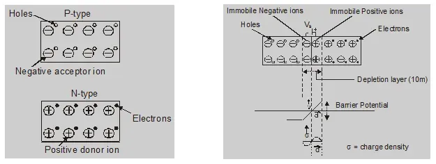
Depletion layer:
There is a barrier near a junction that opposes the flow of charge carrier is known as depletion layer width of the depletion layer is in micrometer order.
Potential Barrier:
Potential developed in depletion layer is called P.B.
P-side is at lower potential and N-side is at higher potential.
P.B. for Ge 0.3 volt
P.B. for Si 0.7 volt
Electric field:
Electric field due to P.B.
$E=\frac{V}{d}$
For Ge
$E=\frac{0.3}{10^{-6}}$
$=3 \times 10^{5} \mathrm{~V} / \mathrm{m}$
order
$\mathrm{E} \approx 10^{5} \mathrm{~V} / \mathrm{m}$
the direction of E due to P.B. N to P-side
P-N Junction with forward bias :
When the Positive terminal of a battery is connected to the P side and the negative terminal to the N side. Then PN Junction is in forwarding Bias
Forward bias reduces the potential barrier. More charge carriers diffuse across the junction.
Special Point:
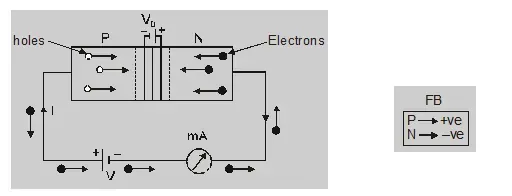
- Potential barrier reduces
- Width of the depletion layer decreases
- P-N junction offers low resistance in forwarding bias.
- Forward current flow in a circuit
- The forward characteristic curve is shown in the figure.
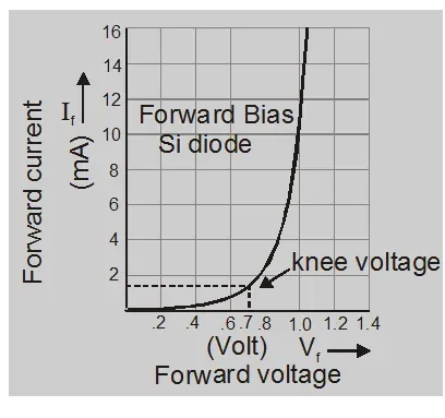
- Forward dynamic resistance $r_{f}=\frac{\Delta V_{f}}{\Delta I_{f}} \cong 100 \Omega$
- Knee or cut in voltageGe 0.3 VSi 0.7 V
- Dependence of forward current on bias voltage $\mathrm{I}=\mathrm{I}_{0}\left[\mathrm{e}^{\frac{\mathrm{qV}}{\mathrm{kT}}}-1\right]$$\mathrm{e}^{\frac{\mathrm{qV}}{\mathrm{kT}}}>>1$
$I \approx I_{0} e^{\frac{+q V}{k T}}$ (Approximate exponential growth)
I = Forward current
$\mathrm{I}_{0}$ = reverse saturation current
k = Boltzman constant
q = charge of electron
V = forward voltage
T = temperature
P-N junction with reverse bias:
When the positive terminal of a battery is connected to the N-side and the negative terminal is connected to the P-side. Holes in the P-region are attracted towards the negative terminal and the electrons in the N-region are attracted towards the positive terminal.
Special Point:
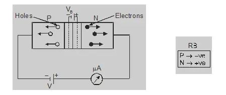
- The depletion layer increases for reverse biased.
- Potential barrier increases
- The reverse characteristic curve is shown in figure
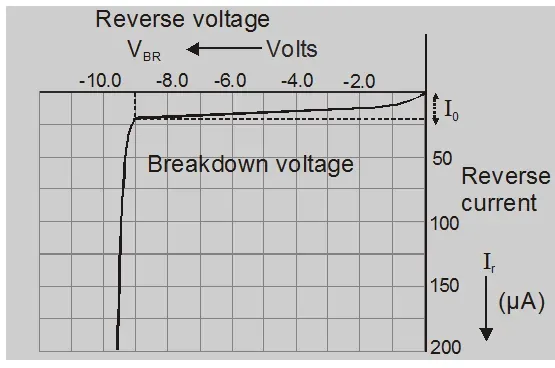
- Very little current called reverse saturation current flows due to minority carrier flow.For Silicon = $10^{-9}$ AFor Germanium = $10^{-6}$ A
- In reverse biased condition, junction behaves as a capacitor of few picofarads.
- In reverse biased condition, junction behaves like high resistive material between two regions.
- In reverse biased P-N diode behaves like an insulator.
- Reverse resistance
$\mathrm{R}_{\mathrm{B}}=\frac{\Delta \mathrm{V}_{\mathrm{B}}}{\Delta \mathrm{I}_{\mathrm{B}}} \cong 10^{6} \Omega$$\frac{R_{B}}{R_{f}}=10^{3}$ : 1 for Geand
$\frac{R_{B}}{R_{f}}=10^{4}$ : 1 for Si - Dependence of reverse current on bias volt.
$\mathrm{I}_{\mathrm{r}}=\mathrm{I}_{0}\left[\mathrm{e}^{-\frac{\mathrm{q} \mathrm{V}}{\mathrm{kT}}}-1\right]$$\mathrm{e}^{-\frac{\mathrm{qV}}{\mathrm{kT}}}<<1$$\mathrm{I} \cong-\mathrm{I}_{0}$
Here $\mathrm{I}_{\mathrm{r}}$ = reverse current
$\mathrm{I}_{0}$ = reverse saturation current
V = applied voltage
q = charge of electron
T = temperature in kelvin
Special Point
- The diffusion current in the p-n junction is greater than the drift current in magnitude if the junction is forward biased.
- A hole diffuses from the p-side to the n-side in a p-n junction. This means that a bond is broken on the n-side and the electron freed from the bond jumps to a broken bond on the p-side to complete it.
So, that's all from this article. I hope you get the idea about what is P-N junction. If you enjoyed this article then please leave your thoughts in the comments section down below.
Also, read
What is Fermi energy level in semiconductors
To watch Free Learning Videos on physics by Saransh Gupta sir Install the eSaral App.
Team eSaral
eSaral Academic and Editorial Team
Team eSaral is the collective author profile for educational content created by eSaral’s teachers and academic contributors. The team draws on expertise from IIT graduates, doctors, experienced educators and subject specialists to develop resources for JEE, NEET and school students. Our articles aim to explain concepts clearly and help students study with confidence.
Related Posts

Plant Cell Diagram: Labelled Structure, Parts and Functions
Simple, labelled plant cell diagram with parts and functions. Covers plant cell structure for Class 6, 7, 8, 9, 10 and 11 students, CBSE-aligned.

Saransh Gupta Sir's Visit to IIT Patna: Hostel Life, Placements & Lessons for JEE Aspirants
Inside Saransh Gupta Sir's IIT Patna visit — hostel life, the library, placements, internships, and real advice for JEE aspirants from students living the IIT dream.
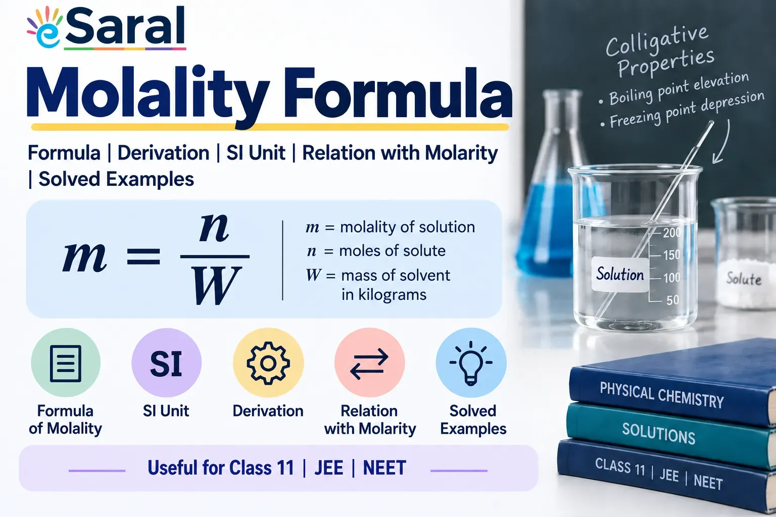
Molality Formula: Formula for Molality, Derivation & Solved Examples
Molality formula is $m = \dfrac{n}{W}$. Learn the formula of molality, its SI unit, derivation, relation with molarity, and solved examples for Class 11, JEE and NEET.

BITSAT Previous Year Question Paper PDF
Download BITSAT previous year question papers PDF. Get year-wise BITSAT PYQs, memory-based papers, exam pattern, and preparation tips to improve your BITSAT preparation.

Teachers’ Day 2026 at eSaral Gurukul: Celebrating the Bond Between Students, Teachers & Mentors
See how Teachers’ Day 2026 was celebrated at eSaral Gurukul, reflecting the bond among students, teachers, and mentors, and the role of guidance beyond academics.
JEE Advanced Attempts: Can You Give It a Third Time? Rules Explained
JEE Advanced attempts: current rule is 2 consecutive years only: full eligibility criteria, the 2025 third-attempt controversy, and the latest 2026 petition news.

Best JEE Preparation App
Best JEE preparation app for Main & Advanced: AI mock tests, live doubt-solving, thousands of practice questions. JEE preparation app for droppers & Class 11-12.
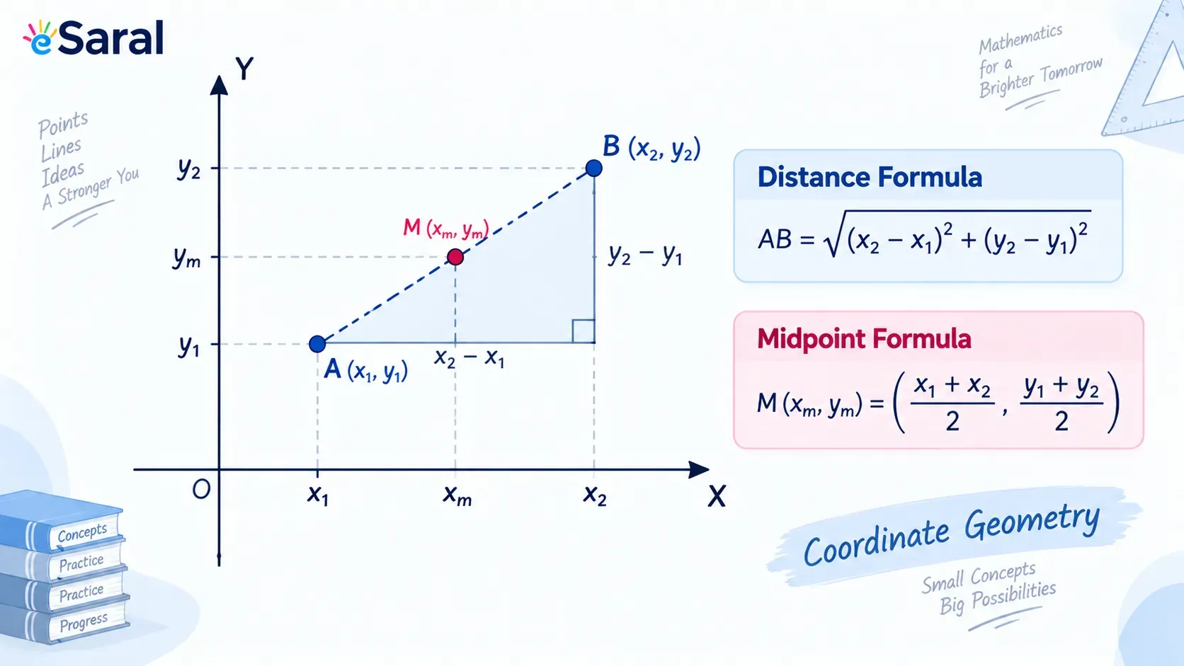
Coordinate Geometry Class 10: Formulas, Notes & Solved Examples
Coordinate geometry class 10: complete CBSE formulas — distance, section, midpoint and area of triangle — with derivation, notes and solved examples.
How to make Notes For JEE Smart Notes Strategy of an AIR 41
Learn how to make notes for JEE the way toppers do — indexing, shorthand, and smart short notes for JEE that cut revision time to just 5–7 days.
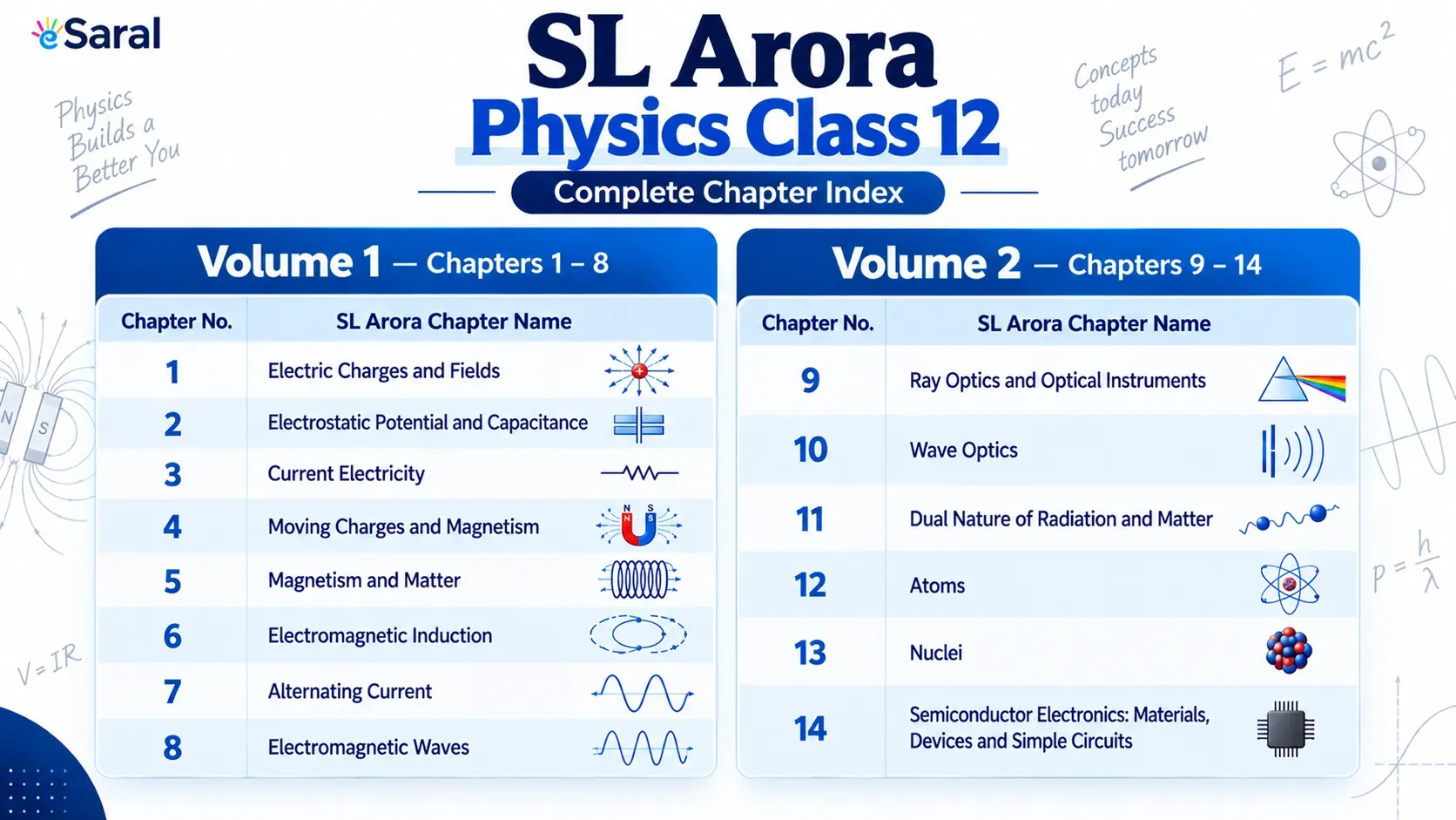
SL Arora Physics Class 12 Index – Chapter List for Volume 1 & 2
SL Arora Physics Class 12 index — complete chapter list for Volume 1 & 2, mapped to NCERT solutions for board, JEE Main, and NEET preparation.