
Working of NPN and PNP transistor - Electronics, Physics - eSaral

eSaral Academic and Editorial Team
Summary
<p>Learn the working of NPN and PNP transistors, current flow mechanisms, common transistor configurations (CB, CE, CC), their characteristics, and the relationship between transistor current gains α, β, and γ.</p>
eSaral › Class 11› Working of NPN and PNP transistor

🚀 Checkout eSaral Courses
Hey, do you want to learn about the Working of NPN and PNP transistor? if yes. Then you are at the right place.
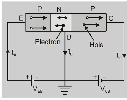
P-N-P Transistor:
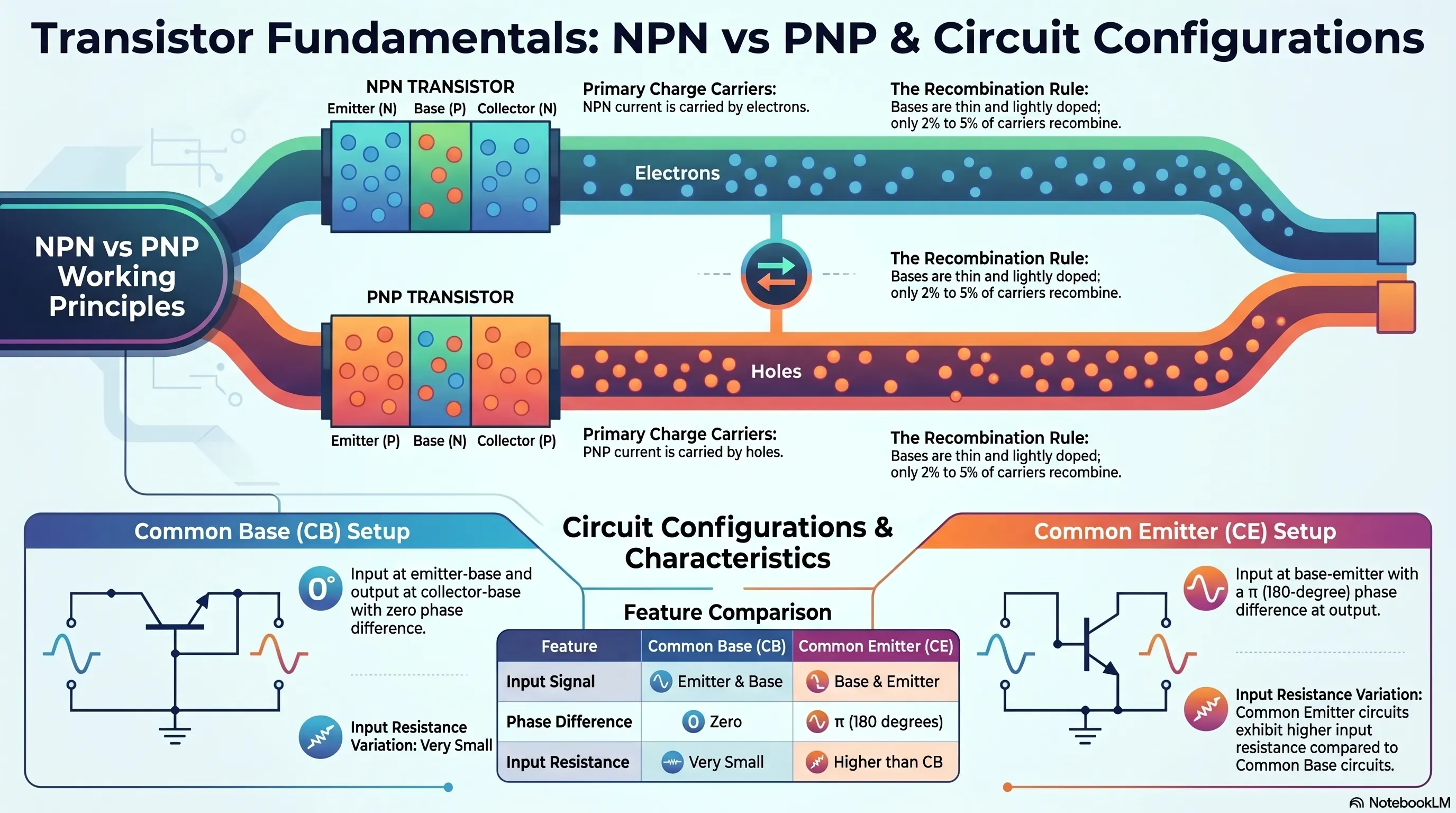
The holes of the P region (emitter) are rippled by the positive terminal of battery $\mathrm{V}_{\mathrm{EE}}$ towards the base. The potential barrier at the emitter junction is reduced as it is forward bias and hence the holes cross this junction and penetrate into the N region. This constitutes the emitter current. The width of the base region is very thin and it is lightly doped and hence only two to five percent of the holes recombine with the free electrons of the N region. This constitutes the base current $\mathrm{I}_{\mathrm{B}}$. which of course, is very small. The remaining holes (95% to 98%) are able to drift across the base and enter into the collector region. This constitutes the collector current.
N-P-N Transistor:
Working:
The electron in the emitter region is rippled from the negative terminal of the battery towards the emitter junction. Since the potential barrier at the junction is reduced due to forward bias and the base region is very thin and lightly doped, electrons cross the p-type base region. A few electrons combine with the holes in P-region and are lost as the charge carriers. Now the electrons in N-region (collector region) readily swept up by the positive collector voltage $\mathrm{V}_{\mathrm{CC}}$.
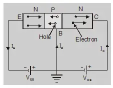
The current conduction in the N-P-N transistor is carried out by electrons.
Transistor configuration
Three types of transistor circuit configuration are
Common base (CB)
Common emitter (CE)
Common collector (CC)
The term ‘Common’ is used to denote the transistor lead which is common to the input and the output.
Common Base Configuration
In this configuration the input signal is applied between emitter and base and the output is taken from collector and base.
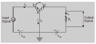
In common base as an amplifier phase difference between input and output is zero.
Characteristics:
Input characteristic:
The curve between emitter current $\mathrm{I}_{\mathrm{E}}$ and emitter base voltage $V_{\mathrm{EB}}$ at constant collector base voltage $\mathrm{V}_{\mathrm{CB}}$ represents the input characteristics. Collector base voltage $\mathrm{V}_{\mathrm{CB}}$ is kept fixed.
- There exist a cut in, offset or threshold voltage $V_{\mathrm{EB}}$ below which the emitter current is very small.
- The emitter current $\mathrm{I}_{\mathrm{E}}$ increases rapidly with small increase in emitter-base voltage $V_{\mathrm{EB}}$. This shows that the input resistance is very small.
Output characteristic:
Curve between collector current $\mathrm{I}_{\mathrm{C}}$ and collector base voltage $V_{\mathrm{CB}}$ at constant emitter $\mathrm{I}_{\mathrm{E}}$ represents the output characteristic.
Common emitter configuration
In this configuration the input signal is applied between base and emitter and the output is taken from collector and emitter.
In common emitter as an amplifier phase difference between input and output is $\pi$.
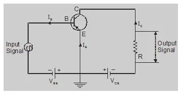
Characteristic
Input characteristics:
The curve between base current $\mathrm{I}_{\mathrm{B}}$ and base emitter voltage $\mathrm{V}_{\mathrm{BE}}$ at constant collector-emitter voltage $\mathrm{V}_{\mathrm{CE}}$ represents the input characteristic.
In this case, $\mathrm{I}_{\mathrm{B}}$ increases less rapidly with $V_{B E}$ as compared to common-base configuration. This shows input resistance of the common-emitter circuit is higher than that of the common-base circuit.
Output characteristic:
The curve between collector current $\mathrm{I}_{\mathrm{C}}$ and collector emitter voltage $V_{C E}$ at constant base current $\mathrm{I}_{\mathrm{B}}$ represents the output characteristic.
Relationship between $\alpha, \beta$ and $\gamma$:
Emitter current $I_{E}=I_{B}+I_{C}$......(1)
divide by $\mathrm{I}_{\mathrm{C}}$ gives, $\frac{\mathrm{I}_{\mathrm{E}}}{\mathrm{I}_{\mathrm{C}}}=\frac{\mathrm{I}_{\mathrm{B}}}{\mathrm{I}_{\mathrm{C}}}+1$
or
$\frac{1}{\alpha}=\frac{1}{\beta}+1$
$\beta=\frac{\alpha}{1-\alpha}$
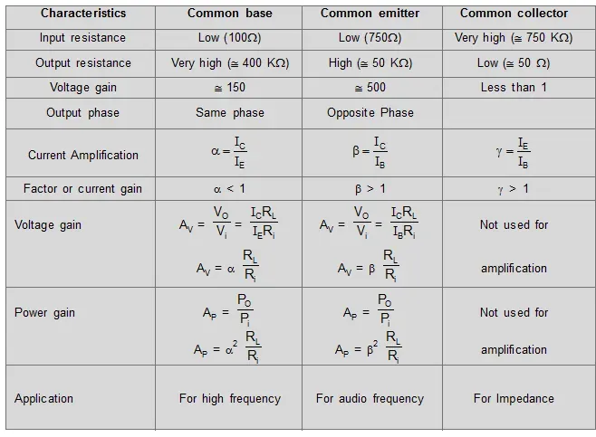
Comparison table between CB, CE and CC configuration
So, that's all from this blog, I hope you get the idea about the Working of NPN and PNP transistor. If you enjoyed this explanation then don't forget to share it with your friends.
Also, read
What is Transistor
To watch Free Learning Videos on physics by Saransh Gupta sir Install the eSaral App.
Frequently Asked Questions
What is the main difference between NPN and PNP transistors?
In an NPN transistor, electrons are the majority charge carriers and conventional current flows from collector to emitter. In a PNP transistor, holes are the majority charge carriers and conventional current flows from emitter to collector. The biasing voltages are also reversed: NPN requires a positive V_CC at the collector, while PNP requires a negative V_CC.
Why is the base of a transistor kept thin and lightly doped?
The base is kept thin (a few micrometres) and lightly doped so that very few charge carriers (electrons in NPN, holes in PNP) recombine within it. This ensures that 95–98% of injected carriers successfully reach the collector, giving the transistor a high current transfer ratio (α close to 1) and therefore a high β.
Which transistor configuration gives the highest voltage gain?
The Common Emitter (CE) configuration gives the highest voltage gain among the three configurations. It also provides significant current gain (β), making it suitable for general-purpose amplification. This is why CE is the most widely used transistor configuration in both analog and digital circuits
What is the relationship between α and β in a transistor?
α and β are related by the equations β = α/(1 – α) and α = β/(1 + β). Since α is always slightly less than 1 (typically 0.95–0.99), the value of β ranges from about 19 to 99 or higher. A high α means very efficient carrier transfer from emitter to collector, resulting in a large β.
What happens when a transistor is in the saturation region?
In the saturation region, both the emitter–base junction and the collector–base junction are forward biased. The transistor conducts heavily; V_CE drops to a very small value (≈ 0.2 V for silicon). The collector current no longer increases with increasing base current. This state is used in switching circuits where the transistor acts as a closed switch.
Team eSaral
eSaral Academic and Editorial Team
Team eSaral is the collective author profile for educational content created by eSaral’s teachers and academic contributors. The team draws on expertise from IIT graduates, doctors, experienced educators and subject specialists to develop resources for JEE, NEET and school students. Our articles aim to explain concepts clearly and help students study with confidence.
Related Posts

Plant Cell Diagram: Labelled Structure, Parts and Functions
Simple, labelled plant cell diagram with parts and functions. Covers plant cell structure for Class 6, 7, 8, 9, 10 and 11 students, CBSE-aligned.

Saransh Gupta Sir's Visit to IIT Patna: Hostel Life, Placements & Lessons for JEE Aspirants
Inside Saransh Gupta Sir's IIT Patna visit — hostel life, the library, placements, internships, and real advice for JEE aspirants from students living the IIT dream.

Molality Formula: Formula for Molality, Derivation & Solved Examples
Molality formula is $m = \dfrac{n}{W}$. Learn the formula of molality, its SI unit, derivation, relation with molarity, and solved examples for Class 11, JEE and NEET.

BITSAT Previous Year Question Paper PDF
Download BITSAT previous year question papers PDF. Get year-wise BITSAT PYQs, memory-based papers, exam pattern, and preparation tips to improve your BITSAT preparation.

Teachers’ Day 2026 at eSaral Gurukul: Celebrating the Bond Between Students, Teachers & Mentors
See how Teachers’ Day 2026 was celebrated at eSaral Gurukul, reflecting the bond among students, teachers, and mentors, and the role of guidance beyond academics.
JEE Advanced Attempts: Can You Give It a Third Time? Rules Explained
JEE Advanced attempts: current rule is 2 consecutive years only: full eligibility criteria, the 2025 third-attempt controversy, and the latest 2026 petition news.

Best JEE Preparation App
Best JEE preparation app for Main & Advanced: AI mock tests, live doubt-solving, thousands of practice questions. JEE preparation app for droppers & Class 11-12.
Coordinate Geometry Class 10: Formulas, Notes & Solved Examples
Coordinate geometry class 10: complete CBSE formulas — distance, section, midpoint and area of triangle — with derivation, notes and solved examples.

How to make Notes For JEE Smart Notes Strategy of an AIR 41
Learn how to make notes for JEE the way toppers do — indexing, shorthand, and smart short notes for JEE that cut revision time to just 5–7 days.
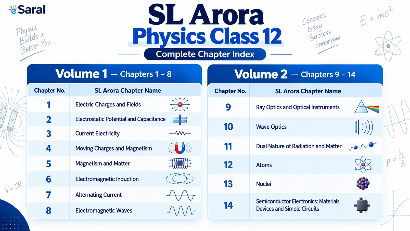
SL Arora Physics Class 12 Index – Chapter List for Volume 1 & 2
SL Arora Physics Class 12 index — complete chapter list for Volume 1 & 2, mapped to NCERT solutions for board, JEE Main, and NEET preparation.